.png)
Milling depaneling component-to-edge clearance is one of the most frequently debated topics between PCB designers, SMT engineers, and manufacturing teams. Everyone wants smaller boards, higher density, and lower cost—but routing physics does not disappear just because layouts become tighter.
So, how close can components realistically be to the PCB edge when using milling depaneling? The answer is not a single number. It depends on how manufacturers define acceptable yield, as well as their process control standards and risk tolerance in real production.
This article shares experience-based insights from global SMT lines, focusing on manufacturability, cost impact, and practical design–process coordination rather than theoretical limits.
🔍 Why Edge Clearance Becomes a Critical Question
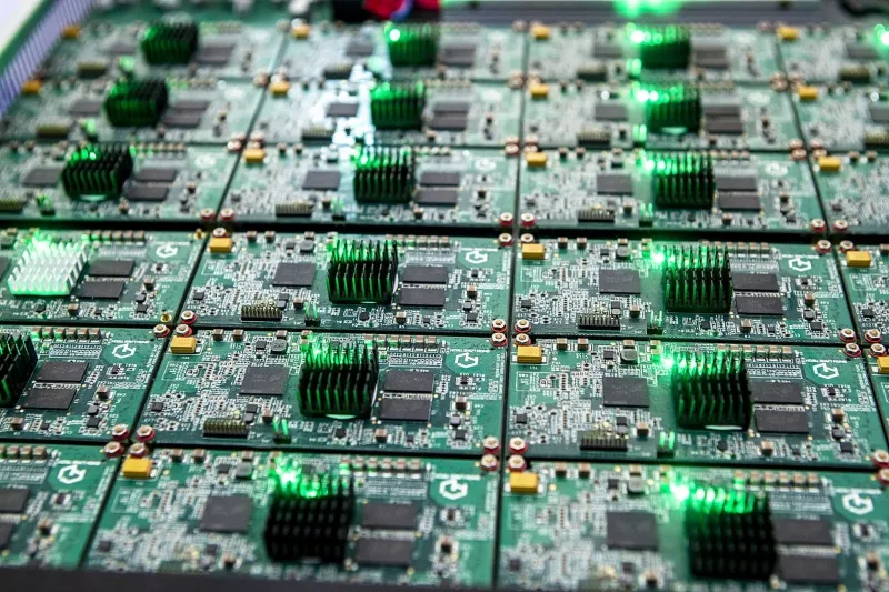
As PCBAs grow denser, edge space is often sacrificed first. However, insufficient clearance can lead to:
- Cracked MLCCs from routing vibration
- Solder joint microfractures near board edges
- Cosmetic damage rejected by downstream inspection
- Hidden reliability risks that appear only after thermal cycling
Many issues are discovered too late—after tooling is already released.
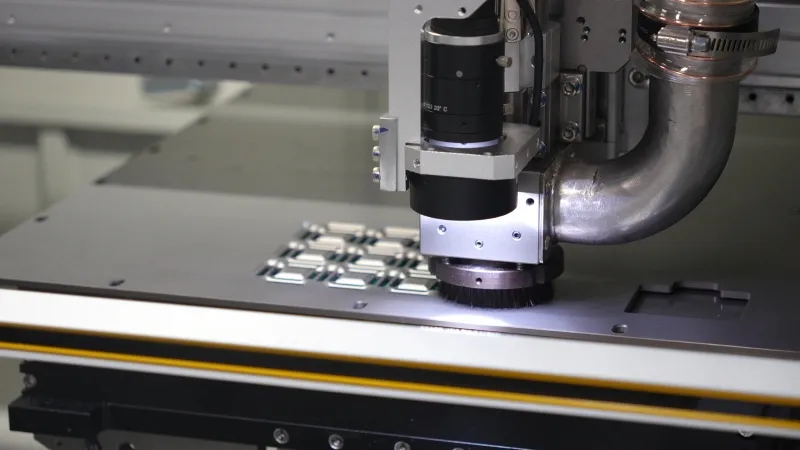
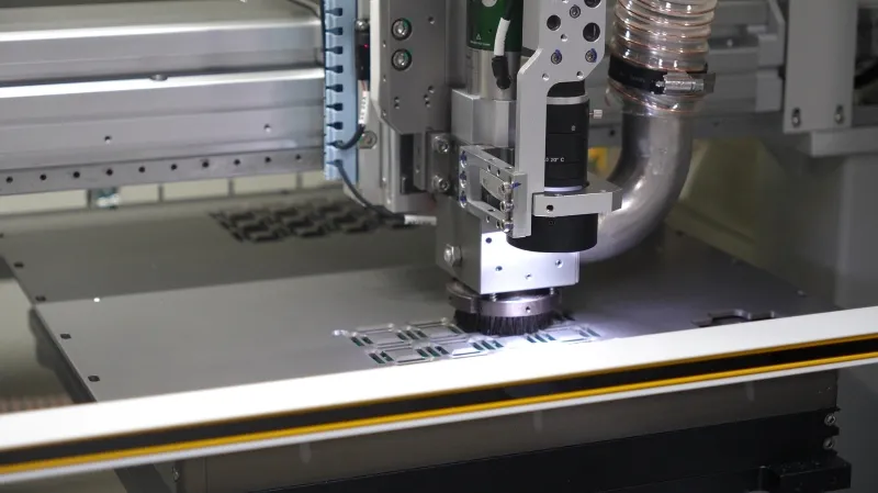
⚙️ What Happens Physically During Milling Depaneling
Milling depaneling removes material mechanically, which introduces:
- Lateral cutting forces
- Localized vibration at the board edge
- Heat and micro-stress in copper and laminate
Even with a stable system, the PCB edge is not a “zero-stress zone.” Components placed too close together will feel that energy.
📏 Common Clearance Ranges Seen in Production
Based on EMS and OEM field data, typical guidance looks like this:
- ≥ 1.0 mm: Generally low risk for most components
- 0.8–1.0 mm: Feasible with controlled parameters and good fixturing
- 0.5–0.8 mm: Requires careful validation, especially for MLCCs
- < 0.5 mm: High risk unless special routing strategies are used
These are not hard rules—but probability curves. The closer the component, the narrower the process window.
🧠 User Pain Point: Design vs. Manufacturing Reality
A common conflict appears when:
- PCB layout is finalized for electrical performance
- Depaneling is considered only at the NPI or pilot stage
- Manufacturing is asked to “make it work.”
This often leads to conservative routing speeds, lower throughput, or added inspection steps—raising cost indirectly.
🛠️ Process Techniques That Allow Tighter Clearances
Factories achieving tighter edge spacing often rely on combined strategies:
- Reduced step-down depth during routing
- Optimized cutter geometry for low lateral force
- Full-area vacuum support to prevent board flex
- Multi-pass routing instead of aggressive single cuts
In several Seprays-supported projects, these adjustments allowed reliable depaneling at ~0.6 mm clearance without yield loss—after validation trials.
📉 Cost Perspective: Clearance vs. Total Manufacturing Cost
Placing components closer to the edge may reduce PCB size, but it can increase hidden costs:
- Slower routing cycles
- Higher tool wear
- Increased inspection and SPC monitoring
- Risk of latent failures in field use
Some automotive programs found that adding 0.2 mm of clearance reduced total lifecycle cost more than shrinking the PCB outline.

🏭 Case Insight: Industrial Control Board
An industrial electronics manufacturer faced repeated edge-related MLCC cracking at 0.5 mm clearance. After reviewing routing force data and fixture flatness, they adjusted the depaneling strategy and achieved stable production—but only after multiple trials and process locks.
The key lesson: tight clearance is possible, but it must be engineered—not assumed.
🌍 Aligning with Global Manufacturing Expectations
In high-reliability sectors, engineers increasingly review depaneling clearance during DFM. Edge distance is no longer just a layout detail—it is part of process qualification and audit documentation.
Early collaboration between design and depaneling specialists significantly reduces late-stage compromises.
💬 Why Choose Seprays Group?
Seprays Group works closely with EMS and OEM teams to evaluate component-to-edge risk in milling depaneling—combining machine capability, fixturing strategy, and real production data. Our approach helps customers achieve compact designs without sacrificing yield or long-term reliability.
If you would like to review your PCB layout or validate edge clearance limits for milling depaneling, please feel free to contact us.
WhatsApp: +8618929266433
E-mail: sales@seprays.com