.png)
 Japanese
  English
  Spanish
  Korean
  Russian
  Chinese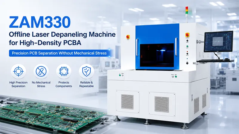
ZAM330 Offline Laser Depaneling Machine is becoming a practical choice for manufacturers producing high-density PCBAs where even slight mechanical stress can affect long-term product reliability.
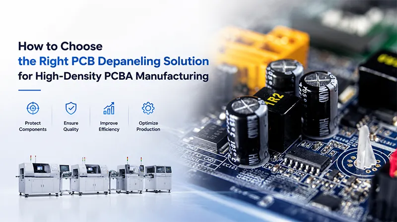
As electronic devices continue to shrink while integrating more functions, PCB layouts have become increasingly compact. Manufacturers place components closer to board edges, adopt more multilayer designs, and integrate expensive ICs or optical modules, leaving little room for processing errors.
Many manufacturers have already invested in high-speed SMT lines and AOI systems. Yet, one production step still deserves more attention—PCB depaneling.
The final separation process may only take seconds, but it can determine whether a finished product performs reliably for years.
This article shares practical observations from modern electronics manufacturing, explains where laser depaneling fits, and discusses why more engineering teams are reconsidering traditional separation methods.
🔍 Why High-Density PCBA Changes the Rules
Ten years ago, many PCB assemblies had generous spacing between routing lines and components.
Today, the situation is very different.
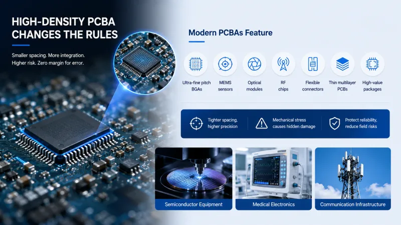
Modern PCBAs often feature:
- Ultra-fine pitch BGAs
- MEMS sensors
- Optical modules
- RF communication chips
- Flexible connectors
- Thin multilayer PCB materials
- High-value semiconductor packages
As component spacing decreases, manufacturing tolerance becomes increasingly critical.
Mechanical force that once caused no visible issues may now create microscopic cracks inside solder joints or PCB layers.
These defects rarely appear during production testing.
Instead, they often become field failures months after products reach customers.
For industries such as semiconductor equipment, medical electronics, and communication infrastructure, this risk is difficult to accept.
⚠️ Hidden Problems Traditional Depaneling May Introduce
Not every PCB requires laser cutting.
For simple V-cut panels with large component clearances, conventional depaneling remains a practical option.
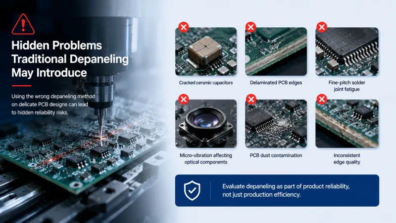
However, manufacturers producing high-density PCBAs often report challenges such as:
- Cracked ceramic capacitors
- Delaminated PCB edges
- Fine-pitch solder joint fatigue
- Micro-vibration affecting optical components
- PCB dust contamination
- Inconsistent edge quality
Interestingly, many of these problems are not caused by poor equipment.
Instead, they result from applying the wrong depaneling method to increasingly delicate PCB designs.
This explains why more engineering teams now evaluate depaneling as part of product reliability rather than simply production efficiency.
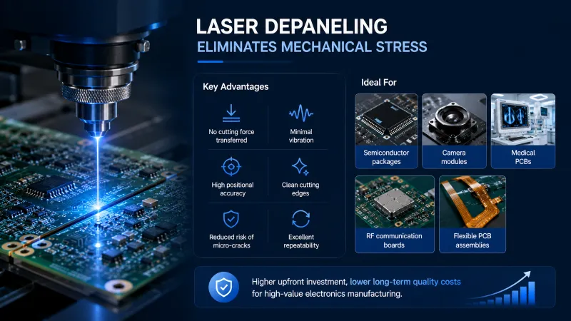
⚡ Why Laser Depaneling Eliminates Mechanical Stress
Unlike milling cutters or saw blades, laser depaneling removes material through a highly controlled laser beam.
There is virtually no physical contact between the cutting tool and the PCB.
This creates several practical advantages.
- No cutting force transferred to nearby components
- Minimal vibration
- High positional accuracy
- Clean cutting edges
- Reduced risk of micro-cracks
- Excellent repeatability
This approach is particularly valuable for:
- Semiconductor packages
- Camera modules
- Medical PCBs
- RF communication boards
- Flexible PCB assemblies
Although laser systems generally require higher initial investment, they often reduce long-term quality costs when manufacturing high-value electronics.
🏭 Where the ZAM330 Fits
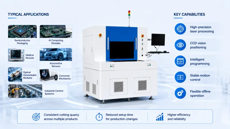
の ZAM330 Offline Laser Depaneling Machine is designed for manufacturers requiring high-precision PCB separation without introducing mechanical stress.
Typical applications include:
- Semiconductor packaging
- AI computing modules
- Medical electronic devices
- Automotive sensors
- Optical communication modules
- Consumer electronics
- Industrial control systems
The system combines:
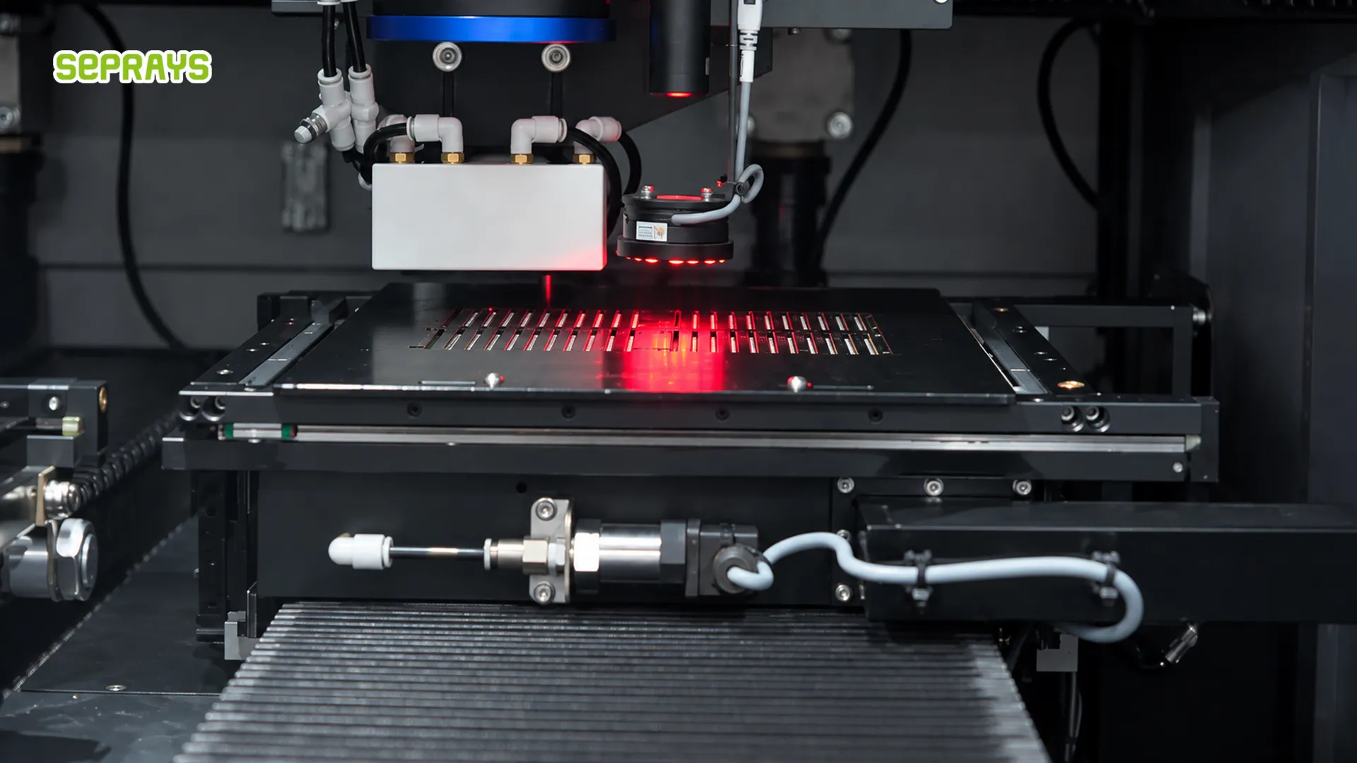
- High-precision laser processing
- CCD vision positioning
- Intelligent programming
- Stable motion control
- Flexible offline operation
These capabilities help manufacturers maintain consistent cutting quality across multiple product types while reducing setup time for production changes.
📊 Comparing Common PCB Depaneling Technologies
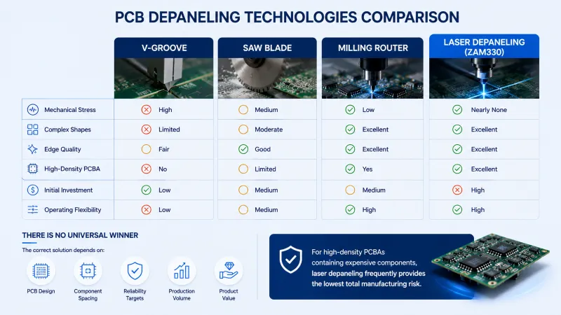
| Method | Mechanical Stress | Complex Shapes | 質感 | High-Density PCBA | Initial Investment | Operating Flexibility |
|---|---|---|---|---|---|---|
| V-Groove | High | Limited | Fair | No | Low | Low |
| Saw Blade | 中 | 緩やかな | Good | Limited | 中 | 中 |
| Milling Router | Low | Excellent | Excellent | あり | 中 | High |
| Laser Depaneling (ZAM330) | Nearly None | Excellent | Excellent | Excellent | High | High |
There is no universal winner.
The correct solution depends on:
- PCB design
- Component spacing
- Reliability targets
- Production volume
- Product value
For high-density PCBAs containing expensive components, laser depaneling frequently provides the lowest total manufacturing risk.
💰 Looking Beyond Equipment Cost
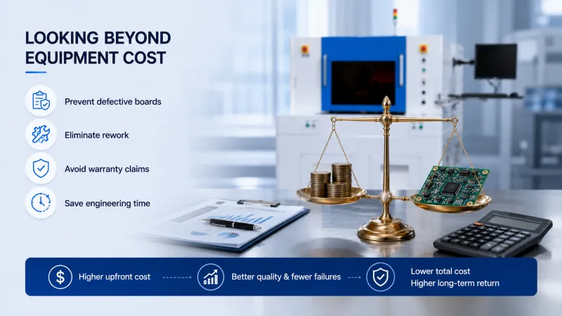
One of the most common purchasing mistakes is comparing machines only by price.
Engineers usually evaluate something different.
They ask:
- How many defective boards can be prevented?
- How much rework can be eliminated?
- How many warranty claims might be avoided?
- How much engineering investigation time can be saved?
When manufacturing expensive semiconductor assemblies, reducing failure rates by only a small percentage may generate significant long-term savings.
In these cases, production quality often delivers a higher return than purchasing the lowest-cost equipment.
🌍 A Real Example: Semiconductor Manufacturer Improves Yield
An overseas semiconductor manufacturer producing high-density communication modules experienced an unusual problem.
Electrical testing showed excellent yields.
However, several customers later reported intermittent failures after products entered service.
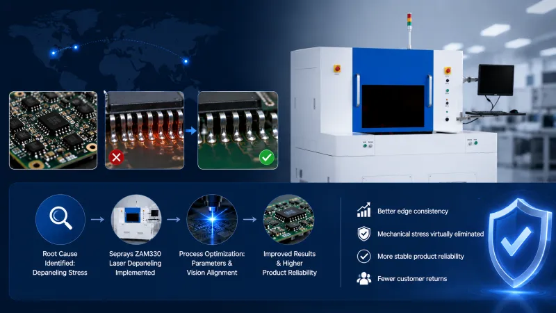
After reviewing SMT, soldering, and inspection processes, engineers eventually focused on PCB separation.
Microscopic analysis revealed that slight mechanical stress during depaneling was affecting solder joints near fine-pitch ICs.
Following process evaluation, the manufacturer introduced the Seprays ZAM330 Offline Laser Depaneling Machine for selected high-value product lines.
After optimizing cutting parameters and vision alignment:
- PCB edge consistency improved.
- Mechanical stress was virtually eliminated.
- Product reliability became more stable.
- Customer returns related to depaneling defects decreased noticeably over subsequent production cycles.
The most important lesson was not simply switching to laser technology.
It was selecting a depaneling process that matched the product’s reliability requirements.
🧠 Lessons Engineers Often Learn Too Late
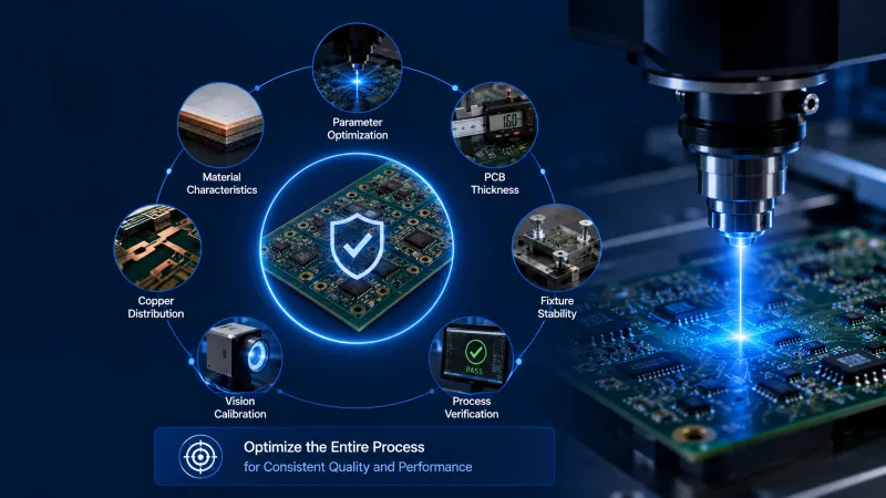
Laser accuracy alone does not guarantee excellent results.
Successful implementation also depends on:
- Proper laser parameter optimization
- Material characteristics
- PCB thickness
- Copper distribution
- Fixture stability
- Vision calibration
- Process verification
Ignoring any one of these factors may reduce overall performance.
The best results come from optimizing the entire process rather than focusing on a single machine specification.
🌱 Why More Manufacturers Are Re-Evaluating Depaneling
Several industry trends are changing how engineers select production equipment.
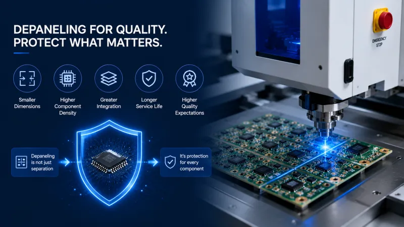
Products continue moving toward:
- Smaller dimensions
- Higher component density
- Greater functional integration
- Longer service life
- Higher quality expectations
As a result, depaneling is no longer viewed as a simple finishing process.
It has become part of product quality assurance.
The goal is not only to separate PCB panels.
The goal is protecting every component already assembled on the board.
💡 Choosing the Right Technology Starts with the Product
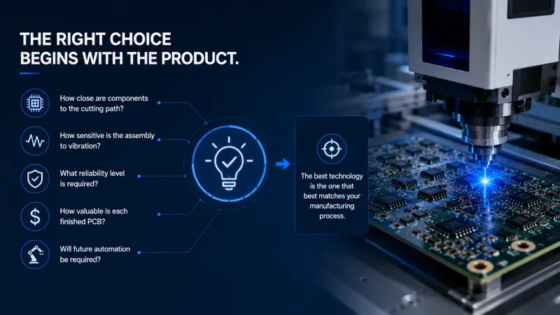
Before investing in new equipment, manufacturers should first evaluate several practical questions.
- How close are components to the cutting path?
- How sensitive is the assembly to vibration?
- What reliability level is required?
- How valuable is each finished PCB?
- Will future automation be required?
The answers usually provide a clearer direction than comparing equipment specifications alone.
In many cases, the best technology is not the most advanced.
It is the one that best matches the manufacturing process.
Why Choose Seprays Group?
For more than 30 years, Seprays Group has specialized in PCB/FPC depaneling technology, helping manufacturers improve precision, efficiency, and long-term production reliability.
Seprays Group has been dedicated to PCB/FPC depaneling technology for over three decades, providing a full range of solutions—including milling-cutter depanelers, laser depanelers, V-groove depanelers, punching depanelers, and automated handling systems. Our equipment is trusted by leading manufacturers, including Foxconn, Flextronics, State Grid, Luxshare, Compal, Wistron, China Electronics, Quanta, CRRC, China Aerospace, OPPO, ZTE, and Bosch. These solutions are deployed in factories across China and worldwide, supporting industries such as semiconductors, automotive electronics, medical devices, consumer electronics, industrial automation, and communications.
Beyond supplying equipment, Seprays works closely with customers to evaluate PCB design, production capacity, reliability goals, and future automation plans. From standalone laser depaneling machines to fully integrated automated production lines, our engineering team helps manufacturers build solutions tailored to real manufacturing challenges.
If you are looking for a reliable laser depaneling solution for high-density PCBA production, please feel free to contact us.
WhatsApp: +8618929266433
Eメール: sales@seprays.com
FAQ
1. What types of PCBs are best suited for the ZAM330 Offline Laser Depaneling Machine?
The ZAM330 is ideal for high-density PCBAs, semiconductor packages, medical electronics, RF modules, optical communication boards, flexible PCBs, and other products where mechanical stress must be minimized.
2. Why choose laser depaneling instead of a milling router?
Laser depaneling eliminates mechanical contact during cutting, making it especially suitable for assemblies with fine-pitch components, delicate solder joints, and high-value electronic devices.
3. Does laser depaneling improve long-term product reliability?
Yes. By avoiding cutting force and vibration, laser depaneling can reduce the risk of micro-cracks, component damage, and hidden defects that may lead to field failures.
4. Is the ZAM330 suitable for low-volume and high-mix production?
Yes. Its offline programming, CCD vision positioning, and flexible process setup allow manufacturers to switch efficiently between different PCB models while maintaining consistent cutting quality.
5. How should manufacturers decide whether laser depaneling is the right choice?
Instead of focusing only on equipment cost, evaluate PCB complexity, component spacing, reliability requirements, product value, production volume, and future automation plans. For high-density, high-value assemblies, laser depaneling often provides the best balance of quality, precision, and long-term manufacturing value.