Japanese
 English
 Spanish
 Korean
 Russian
 Chinese
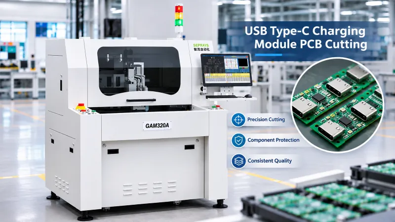
USB Type-C charging module PCB cutting looks simple until a small board fails inspection.
A charging module may be only a few centimeters wide, yet its connector, solder joints, and copper traces leave little room for cutting errors.
For SMT manufacturers, the real challenge is not separating the PCB quickly. It is maintaining consistent edge quality without damaging components that have already passed through assembly.
So, how should engineers approach precision depaneling?
🔍 Why Are Type-C Charging Boards Difficult to Cut?
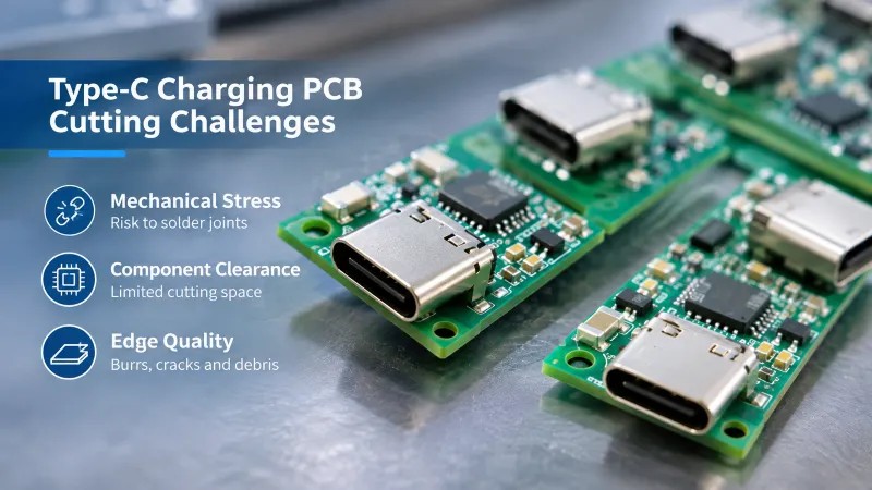
USB-C charging modules often combine compact PCB layouts with connectors positioned close to the board edge.
Three problems deserve attention:
- Mechanical stress: Excessive bending may affect connector solder joints.
- Component clearance: Cutting tools need sufficient space around nearby components.
- Edge quality: Burrs, cracks, and debris can affect downstream assembly.
A board that looks acceptable immediately after cutting may still require electrical or mechanical validation.
That is why visual inspection alone is not enough.
⚙️ How Does the GAM320A Cutting Process Work?
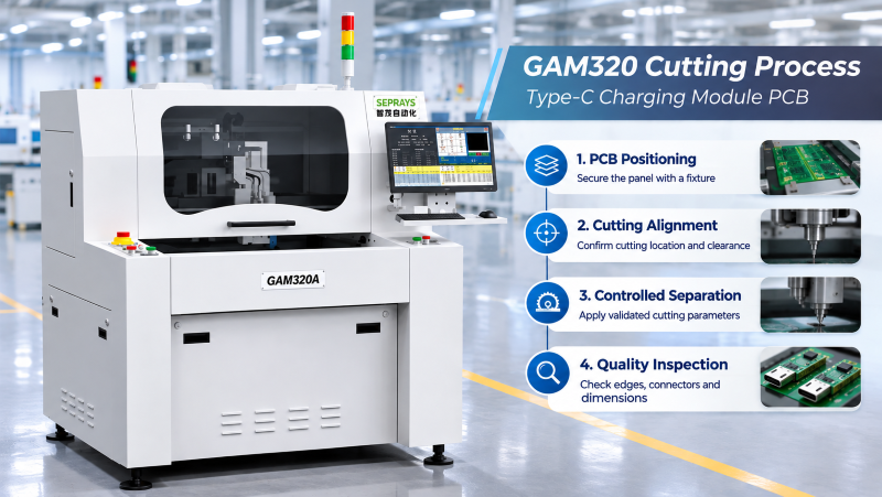
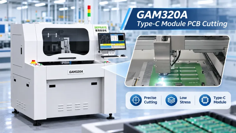
の SEPRAYS GAM320A Cutting-Type Charging Head Module (Type-C) demonstrates a cutting-oriented approach to separating compact charging-module boards.
A practical evaluation follows four stages:
- PCB positioning: Secure the panel using a suitable fixture.
- Cutting alignment: Confirm the cutting location and component clearance.
- Controlled separation: Apply validated cutting parameters.
- Quality inspection: Check edges, connector areas, and separated-board dimensions.
The important detail is repeatability.
A successful demonstration proves that a board can be cut. A production trial must establish whether the process remains consistent across repeated cycles.
The exact GAM320A cutting mechanism, tolerance, and cycle-time specifications should be confirmed against the manufacturer’s technical documentation.
🏭 Which Cutting Method Is Best for Charging Modules?
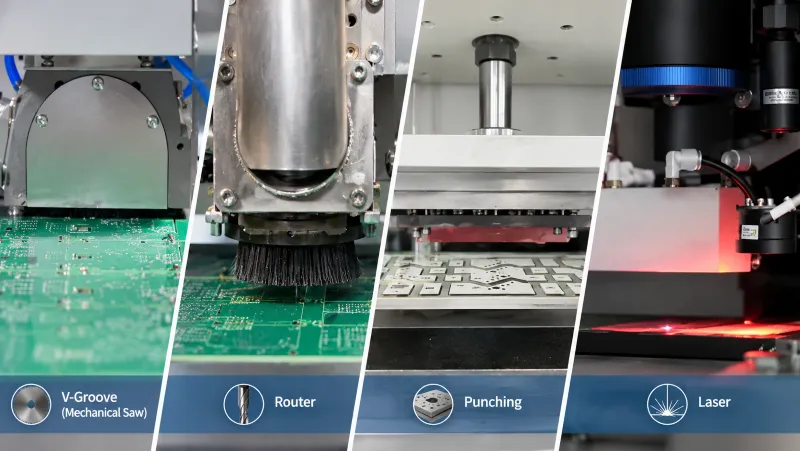
Different PCB designs require different separation methods.
| Method | Advantage | Limitation |
|---|---|---|
| Cutting-type separation | Efficient for compatible panel designs | Requires stress and clearance validation |
| PCB routing | Flexible cutting paths | Tool wear and dust |
| Laser cutting | Non-contact separation | Thermal effects and material compatibility |
| V-groove separation | Efficient for pre-scored panels | Limited to suitable PCB designs |
Laser cutting is not automatically the best choice for every USB-C module.
If a mechanical cutting process meets connector-stress and edge-quality requirements, it may offer a more economical solution.
The final decision should follow actual sample testing.
💰 What Does Precision Cutting Really Cost?
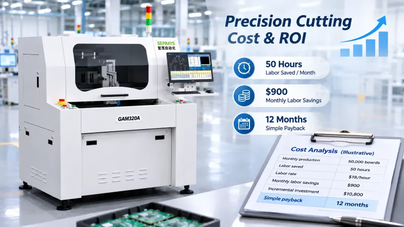
Consider a hypothetical factory producing 50,000 charging-module boards monthly.
Suppose improved fixtures and automated handling save 50 labor hours per month.
| Cost Factor | Illustrative Value |
|---|---|
| Monthly production | 50,000 boards |
| Labor saved | 50 hours |
| Labor rate | $18/hour |
| Monthly labor savings | $900 |
| Incremental investment | $10,800 |
| Simple payback | 12 months |
These figures exclude maintenance, consumables, scrap reduction, downtime, and financing.
The unexpected lesson?
A more expensive machine does not necessarily deliver a better return.
For compact, stable PCB designs, process reliability and fixture efficiency may matter more than maximum cutting speed.
🌍 A Practical Scenario: Guadalajara, Mexico
Imagine an EMS manufacturer in Guadalajara, Jalisco, Mexico, producing compact USB-C charging modules.
The factory experiences occasional connector-area defects after manual board separation.
Its engineers consider evaluating a SEPRAYS GAM320A cutting solution.
Instead of focusing on machine speed, they establish measurable acceptance criteria:
- Inspect board edges and connector solder joints.
- Compare defect rates before and after separation.
- Measure complete cycle time, including handling.
- Check fixture repeatability and maintenance access.
The team may discover that reducing mechanical stress matters more than saving a fraction of a second per cut.
This is an illustrative scenario, not a documented SEPRAYS customer installation. Actual results require sample testing and inspection data.
🧪 What Should Buyers Test Before Ordering?
A supplier demonstration should answer practical engineering questions.
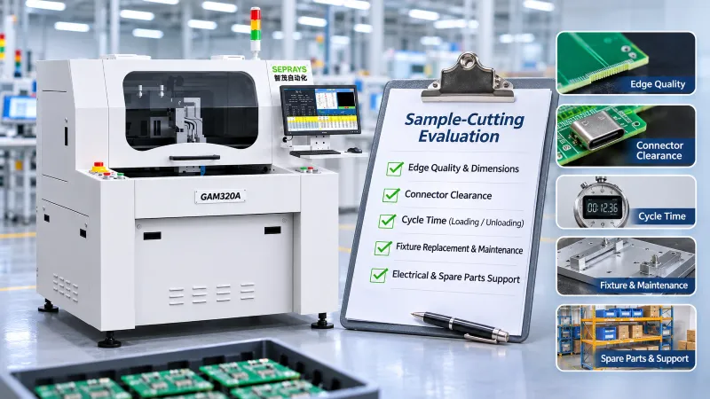
Ask for a sample-cutting evaluation covering:
- PCB edge quality and dimensional consistency.
- Connector clearance and solder-joint integrity.
- Actual cycle time, including loading and unloading.
- Fixture replacement and maintenance requirements.
- Electrical requirements, spare parts, and overseas support.
For stress-sensitive designs, consider strain measurements or appropriate reliability testing.
A machine should pass agreed acceptance criteria before a purchase decision.
📖 Why SEPRAYS Focuses on Precision Depaneling
SEPRAYS Group began developing PCB/FPC depaneling technology in 1993.
The manufacturing challenge has always extended beyond cutting.
After SMT assembly, a small charging board already contains valuable components and completed solder joints. A poor separation process can compromise that work.
This is why SEPRAYS has developed routing, laser, V-groove, punching, and automated material-handling solutions.
The GAM320A Type-C application reflects the same engineering priority: matching the separation process to the actual product rather than expecting one machine to suit every PCB.
Precision is not only about a cutting tolerance. It is about protecting the value already built into the board.

⭐ Why Choose SEPRAYS?
With more than 30 years of experience, SEPRAYS Group provides PCB/FPC depaneling and manufacturing automation solutions.
Its portfolio includes milling-cutter depanelers, laser depanelers, V-groove machines, punching equipment, and automated loading, unloading, and handling systems.
According to company-provided information, SEPRAYS has served organizations including Foxconn, Flextronics, State Grid, Luxshare, Compal, Wistron, China Electronics, Quanta, CRRC, China Aerospace, OPPO, ZTE, and Bosch.
Its engineering team evaluates PCB drawings, panel layouts, cutting paths, production volumes, and downstream handling requirements to identify suitable equipment configurations.
Looking for a precision PCB cutting solution for USB Type-C charging modules?
連絡先 SEPRAYS Group to discuss your application, request a machine recommendation, or arrange a PCB sample-cutting evaluation.
WhatsApp: +8618929266433
Eメール: sales@seprays.com
❓ FAQ
1. What is the best cutting method for USB Type-C charging module PCBs?
It depends on PCB material, connector clearance, panel design, and stress requirements. Cutting-type separation, routing, and laser processing may all be suitable after validation.
2. Can PCB cutting damage a USB-C connector?
Yes. Excessive mechanical stress can affect connector solder joints or nearby components. Proper fixturing and validated cutting conditions help reduce this risk.
3. What is the SEPRAYS GAM320A used for?
The GAM320A is presented in the supplied application description as a cutting-type solution for Type-C charging head modules. Its detailed capabilities should be confirmed with SEPRAYS.
4. How can manufacturers measure PCB cutting quality?
Common methods include edge inspection, dimensional measurement, cycle-time recording, and electrical or mechanical reliability testing where appropriate.
5. Can SEPRAYS provide customized PCB cutting solutions?
Yes. SEPRAYS offers multiple depaneling technologies and automation options. Suitability depends on the PCB design, production requirements, and engineering evaluation.