.png)
Seprays Group: Which PCB Depaneling Method Causes the Least Stress?
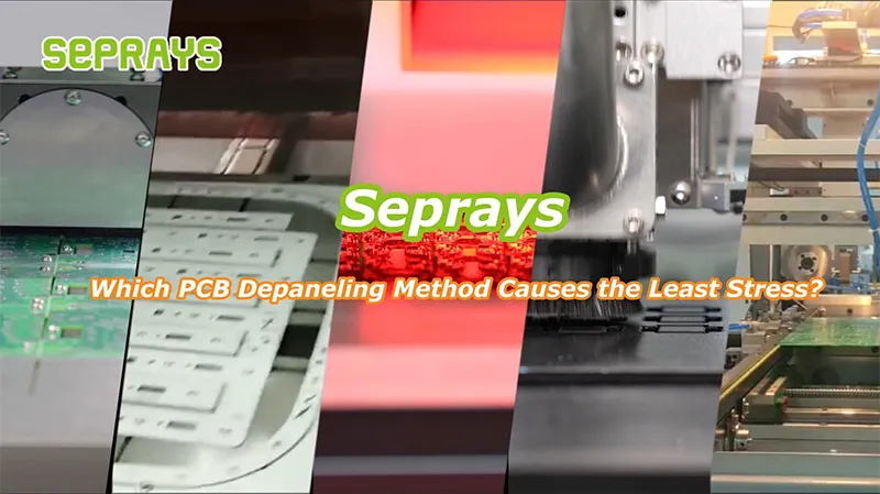
Which PCB depaneling method causes the least stress? For engineers and production managers, this question often arises when dealing with sensitive PCBs. In SMT manufacturing, edge cracks, micro-stress, and component damage can lead to rework, delays, and higher costs. Choosing the right depaneling technique is critical to maintain quality and throughput. 🔧 Understanding Stress in PCB Depaneling Stress in depaneling arises from mechanical force, vibration, or heat. Methods like sawing and punching physically push the board, which can: Reducing these stresses is essential for fragile, high-density, or multi-layer PCBs. ⚡ Comparing Common Depaneling Methods Not all methods affect boards the same way. Here’s a practical overview: Method Stress Level Best […]
Join Us at Productronica China 2026
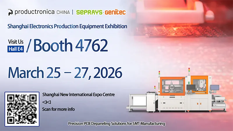
The global electronics manufacturing industry continues to evolve rapidly, driven by increasing demands for precision, efficiency, and automation. As one of the leading events in this field, productronica China brings together innovators, engineers, and manufacturers worldwide. In 2026, SEPRAYS and Genitec will be present at this important exhibition, showcasing advanced solutions designed to address real challenges in SMT production environments. 📍 Where to Find Us We invite you to visit us at: Whether you are exploring new technologies or looking to optimize your current production line, our team will be ready to discuss practical solutions tailored to your needs. ⚙️ What We’ll Be Showcasing At the booth, we will present […]
What Problems Can Saw Blade PCB Depaneling Solve in SMT Manufacturing?
What Problems Can Saw Blade PCB Depaneling Solve in SMT Manufacturing? It’s a question that often comes up when production lines start pushing for higher output but run into bottlenecks at the depaneling stage. In real factory environments, the issue is rarely about technology alone—it’s about stability, cost, and keeping the line moving. 🔍 The Hidden Bottleneck in SMT Lines In SMT manufacturing, most attention goes to placement accuracy and reflow quality. But once boards come off the line, depaneling becomes the next critical step. Common issues include: Saw blade depaneling addresses these problems with a straightforward approach. It keeps things predictable. ⚙️ Solving Throughput Pressure High-volume SMT lines don’t […]
Why Saw Blade Depaneling Is Common in Mass PCB Production
Saw blade depaneling is one of those processes that rarely gets the spotlight, yet it quietly supports high-volume PCB manufacturing every day. If you’ve ever dealt with tight production schedules or cost pressure, you’ve probably seen why this method keeps showing up on factory floors. 🔧 What Makes Saw Blade Depaneling So Widely Used? In mass production, consistency matters more than anything. Saw blade depaneling delivers exactly that. It uses a rotating blade to separate PCBs along straight lines, typically V-grooves. The process is simple, repeatable, and fast. No complex programming.No expensive setup.Just stable throughput. For manufacturers producing thousands—or millions—of identical boards, that reliability becomes a major advantage. ⚙️ Speed […]
Why PCB Router Depaneling Is Widely Used in Electronics Manufacturing
PCB router depaneling remains one of the most common PCB separation methods in electronics manufacturing. Even with newer technologies like laser cutting, many factories still rely heavily on router systems for daily production. Why? Because router depaneling sits in a practical middle ground. It offers flexibility, stable cutting quality, and reasonable operating cost. For many PCB designs, that balance makes it the most reliable choice. In real manufacturing environments, the decision is rarely about technology alone. Engineers care about yield stability, production speed, board design, and long-term reliability. 🔍 Router Depaneling Handles Complex PCB Shapes One of the biggest advantages of router depaneling is its cutting flexibility. Unlike V-cut separation, […]
How Do Engineers Decide If PCB Router Depaneling Is Necessary?
PCB router depaneling is one of the most widely used PCB separation methods in electronics manufacturing. But engineers rarely choose it automatically. In many projects, the decision is made only after reviewing PCB design details, production requirements, and reliability risks. Some boards work perfectly with V-cut separation. Others require laser cutting. In many cases, router depaneling is the most balanced option. So how do engineers actually make that decision in real production environments? 🔍 The First Question Engineers Ask — How Is the PCB Designed? The PCB layout usually determines the depaneling method. Engineers start by checking several key design factors: If the board outline includes curves, internal slots, or […]
Is Laser PCB Depaneling the Best Choice for High-Density PCBA?
Laser PCB depaneling is often discussed when engineers start working with high-density PCBA designs. As boards become smaller and component spacing tighter, traditional mechanical separation methods sometimes reach their limits. Many production teams then begin evaluating laser cutting as an alternative. But is laser depaneling always the best option for high-density PCBA? In practice, the answer depends on board layout, reliability requirements, and production strategy. Let’s look at the issue from a real manufacturing perspective. 🔍 Why High-Density PCBA Changes the Depaneling Challenge High-density PCBA designs are very different from older PCB layouts. Components are packed closer together, and the space near the board edge becomes extremely limited. Common characteristics […]
Laser vs Router PCB Depaneling: Which Method Is Best for Modern PCBA?

Laser vs Router PCB Depaneling is a topic that comes up frequently when production teams start dealing with smaller, denser PCB designs. Years ago, router depaneling handled most boards without issue. But as components moved closer to the edge and product reliability requirements increased, many engineers began reconsidering the cutting method. So which one actually fits modern PCBA production better? The answer depends on board design, component placement, production scale, and cost priorities. Let’s break it down from a practical manufacturing perspective. 🔍 Two Common Depaneling Methods in PCBA Production Both router and laser depaneling are widely used in electronics manufacturing, but they work in very different ways. Router depaneling […]
When Should You Choose Router Depaneling Over V-Cut?
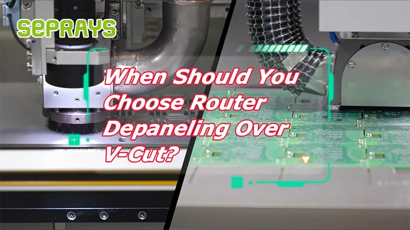
Router depaneling over V-cut is a decision many PCB engineers face sooner or later. At first glance, V-cut looks simple and fast. It works well for many standard panels. But once board designs become more complex, or when component placement moves closer to the edge, router depaneling often becomes the safer choice. This is not about one process being universally better. In real manufacturing environments, the choice usually depends on PCB design constraints, component layout, and long-term yield stability. Let’s walk through the situations where router depaneling makes more sense. 🔍 Understanding the Two Processes Before deciding, it helps to understand how the two methods separate PCBs. V-cut depaneling Router […]
When Should You Choose Laser Depaneling Instead of Router Depaneling?
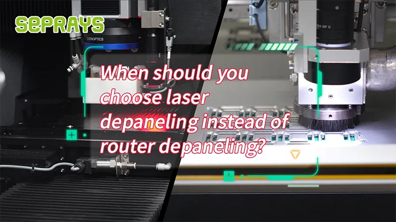
Laser depaneling instead of router depaneling is a question many engineers ask when PCB designs start getting smaller and more complex. In early production stages, router cutting may work well. But as component density increases and reliability requirements tighten, manufacturers often evaluate laser solutions. This article shares practical insights from real production environments—looking at design limitations, cost considerations, and real-world manufacturing challenges. 🔍 Understanding the Two Depaneling Methods Before deciding which one to choose, it’s important to understand how the two processes differ. Router depaneling separates PCBs using a high-speed rotating cutting bit. It physically mills the board along a programmed path. Laser depaneling uses a focused laser beam to […]

