.png)
 Japanese
  English
  Spanish
  Korean
  Russian
  Chinese
Automated Laser PCB Depaneling becomes much more interesting when the PCB is no longer a simple board.
AI servers, semiconductor equipment, automotive electronics, and high-performance computing systems often use boards with dense components, fine traces, unusual outlines, and tighter quality requirements. In these applications, the question is not simply, “How fast can we separate the panel?”
A better question is:
Can the separation process keep up with the board’s accuracy, quality, and automation requirements?
That is where laser processing starts to make practical sense.
🔍 Why AI Hardware Changes the Depaneling Problem
AI hardware is pushing electronics manufacturing toward higher component density and more complex PCB structures.
A small amount of mechanical stress can become a quality concern when components are sensitive or when the board contains fine interconnections.
Traditional mechanical cutting methods can still be highly effective for many applications. But they may not be the first choice when manufacturers need:
- Minimal mechanical stress
- Fine and complex cutting paths
- High positioning accuracy
- Clean edges
- Flexible product changeover
- Inline automation
For these applications, the cutting method needs to be considered together with the entire production process.

⚙️ What Makes Laser Processing Different?
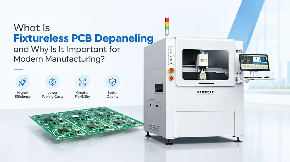
Laser cutting removes material without direct contact between a cutting tool and the PCB.
That changes several things.
There is no milling cutter gradually wearing against the board. There is also no mechanical cutting force in the same way as in router-based separation.
For high-precision electronics, this can be useful when the PCB outline is complex or when component stress needs to be controlled.
The actual result still depends on laser type, wavelength, power, pulse parameters, material, thickness, and cutting path.
In other words, laser does not automatically mean better.
The process still needs to be validated on the actual PCB.

📐 Accuracy Matters More as PCB Density Increases
For modern electronics, positioning errors that were acceptable several years ago may become more noticeable.
A production system may need to recognize the actual PCB position before cutting rather than assuming that every panel arrives in exactly the same location.
Vision-based alignment can help address this problem.
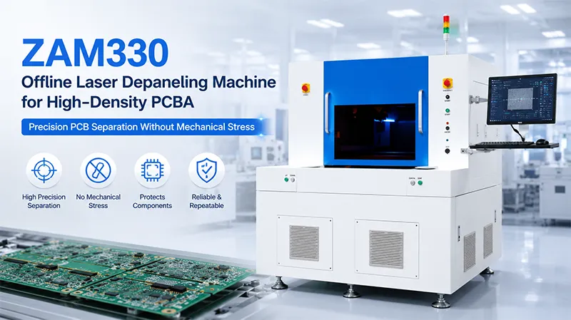
の ZAM330AT/330AD, for example, combines CCD vision and height measurement for automatic alignment. Its specifications also include dual work platforms and a maximum processing area of 300 × 300 mm.
For a production engineer, these details matter more than simply seeing the word “laser” on a machine specification sheet.

🏭 From Standalone Machine to Automated Production Cell
A common mistake is to evaluate a depaneling machine separately from the rest of the production line.
Consider a typical process:
PCB Infeed → Positioning → Vision Alignment → Laser Cutting → PCB Outfeed → Tray Loading
If an operator still needs to manually move every board, the cutting machine may be fast, but the overall process is not truly automated.
The ZAM330AT + ZM620M concept addresses this from a system perspective:
- Automatic PCB infeed
- Vacuum pick and place
- Laser cutting
- Automatic PCB outfeed
- Automatic tray loading
This approach is particularly relevant for factories looking to reduce repetitive handling and improve process consistency.
の ZAM330AT/330AD platform also supports robotic loading and unloading, dual worktables, and MES integration for production data and quality tracking.

📊 Laser vs. Mechanical Depaneling
There is no universal winner.
| Requirement | Laser | Router / Milling |
|---|---|---|
| Mechanical stress | Very low | Higher |
| Complex contours | Excellent | Excellent |
| Tool wear | No cutting-tool wear | Tool replacement required |
| Dust generation | Process-dependent | Higher |
| Straight V-groove boards | Usually unnecessary | Usually unnecessary |
| Flexible product designs | Excellent | Good |
| High-volume production | Excellent when properly configured | Excellent |
The practical choice depends on the PCB.
For a standard FR-4 board with simple routing, a milling solution may be more economical.
For dense electronics, sensitive components, FPCs, or demanding contours, laser processing may justify the additional investment.

💰 What About the Cost?
The purchase price is only one part of the calculation.
Manufacturers should also consider:
Cost per board = equipment + labor + tooling + maintenance + consumables + downtime + quality losses
Laser equipment can have a higher initial investment than some mechanical alternatives.
But that does not automatically make it more expensive over the entire production lifecycle.
For example, a factory producing several high-value PCB models may place greater value on:
- Reduced tooling requirements
- Faster product changeover
- Lower operator involvement
- Stable cutting quality
- Automated material handling
The important number is therefore not simply the machine price.
It is the total cost per acceptable finished board.

🧪 A Practical Semiconductor Manufacturing Scenario
Consider an overseas semiconductor equipment manufacturer producing control boards for different generations of semiconductor processing equipment.
The boards are not identical.
Some have different outlines. Others contain sensitive components positioned close to the cutting path.
The factory initially focused on cutting speed.
After production trials, however, the engineering team found that handling, positioning, and changeover time had a larger impact on throughput than expected.
A Seprays laser depaneling solution could be evaluated in this type of environment, combining precision laser processing with automated handling rather than treating PCB separation as an isolated operation.
For a solution such as the ZAM330AT + ZM620M, the stated machine precision is ±20 μm with repeat precision of ±2 μm, while the process can be configured for automatic loading, cutting, unloading, and tray handling.
These figures should still be verified against the customer’s actual PCB, material, and process conditions before production approval.
That last step is important.
A specification sheet is not a process validation report.

🧩 Where Laser Depaneling Has Limits
Laser technology is not the right answer for every board.
Manufacturers should test:
- PCB material
- 基板厚み
- Copper distribution
- Thermal sensitivity
- Required edge appearance
- 切削速度
- Fume extraction
- Production volume
Different laser wavelengths can also behave differently with different materials.
の ZAM330AT/330AD platform supports optional UV and CO₂ laser configurations, with the product page listing applications including PCBA depaneling, FPC cutting, coverlay window opening, and advanced materials such as LCP, MPI, PI, PET, FR4, and ceramic substrates.
This is why sample testing remains essential before selecting the final process.

🚀 The Bigger Shift: Automation Around the Cut
The interesting development in 2026 is not simply that laser cutting is becoming more precise.
It is that depaneling is increasingly being treated as one connected manufacturing step.
Vision.
Handling.
Cutting.
Inspection.
Tray loading.
MES data.
When these functions work together, manufacturers can reduce the number of manual decisions made during production.
For AI hardware and other high-performance electronics, this may be more valuable than gaining a few seconds from the cutting cycle.

⭐ Why Choose Seprays Group?
With more than 30 years of experience, Seprays Group has focused on PCB and FPC depaneling technology and the practical manufacturing problems behind PCB separation.
Seprays Group has been dedicated to PCB/FPC depaneling technology, providing a full range of solutions—milling-cutter depanelers, laser depanelers, V-groove depanelers, punching depanelers, and automated handling systems. Our equipment is trusted by leading manufacturers, including Foxconn, Flextronics, State Grid, Luxshare, Compal, Wistron, China Electronics, Quanta, CRRC, China Aerospace, OPPO, ZTE, and Bosch. It is used in factories across China and worldwide.
For manufacturers working with AI hardware, semiconductor electronics, automotive electronics, medical devices, or other high-value PCBs, Seprays can evaluate the PCB structure, production requirements, automation needs, and separation method before recommending an appropriate solution.
の ZAM330AT/330AD is an example of Seprays’ laser platform, designed for high-precision PCB and FPC processing with automated handling, vision alignment, dust extraction, cooling, and production-line integration.
Explore the ZAM330AT/330AD Laser Depaneling Solution
If you have a PCB drawing, Gerber file, panel layout, or specific production requirement, please get in touch with us for a process evaluation.
WhatsApp: +8618929266433
Eメール: sales@seprays.com
❓ FAQ
1. Is laser depaneling suitable for AI hardware PCBs?
It can be. Laser processing is particularly useful when manufacturers need low mechanical stress, precise contours, or flexible cutting paths. The actual suitability should be confirmed through PCB sample testing.
2. What is the difference between laser and router depaneling?
A router uses a rotating mechanical cutting tool, while laser processing removes material through a focused laser beam. Router cutting can be highly economical for many FR-4 applications, while laser cutting can be advantageous for complex or stress-sensitive boards.
3. Does laser depaneling completely eliminate PCB damage?
No. Laser processing can significantly reduce mechanical stress, but thermal effects, material characteristics, cutting parameters, and PCB structure still need to be controlled.
4. Can the laser depaneling process be automated?
Yes. Automated systems can combine PCB feeding, vacuum pick-and-place, vision alignment, cutting, unloading, and tray handling. The ZAM330AT + ZM620M configuration is designed around this type of workflow.
5. Should manufacturers choose the machine based on precision specifications alone?
No. Precision is only one factor. Production volume, PCB material, cutting path, cycle time, handling requirements, dust and fume control, maintenance, and total cost per finished board should also be evaluated.