.png)
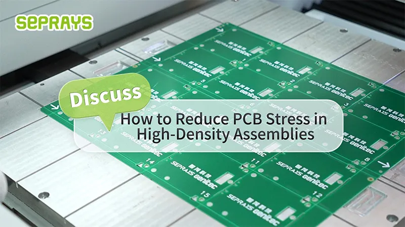
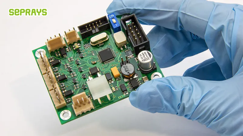
PCB stress has quietly become one of the biggest reliability risks in high-density assemblies.
A board may pass AOI.
The solder joints may look perfect.
Functional testing may even pass.
But hidden mechanical stress inside the PCB can still create long-term failures later.
In 2026, this problem is becoming more common because electronics are getting:
- smaller
- thinner
- denser
- more complex
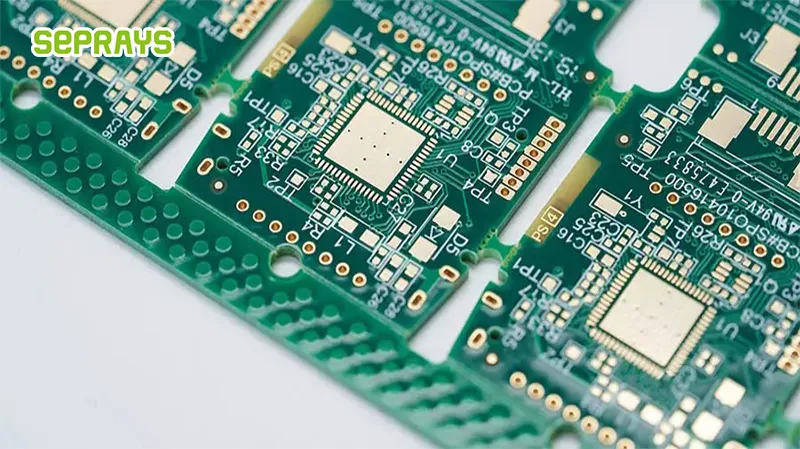
Components are now placed closer to PCB edges.
Multilayer boards are more fragile.
And the depaneling processes that worked years ago may no longer be safe enough.
For manufacturers working with automotive electronics, medical devices, communication modules, semiconductor systems, or industrial control boards, reducing PCB stress is no longer optional.
It directly affects SMT yield and product reliability.
🔍 What Causes PCB Stress in High-Density Assemblies?
PCB stress usually comes from multiple production stages combined.
Common sources include:
- depaneling vibration
- manual handling
- improper fixtures
- board flexing
- thermal expansion
- conveyor pressure
- uneven support during routing
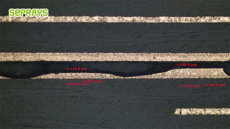
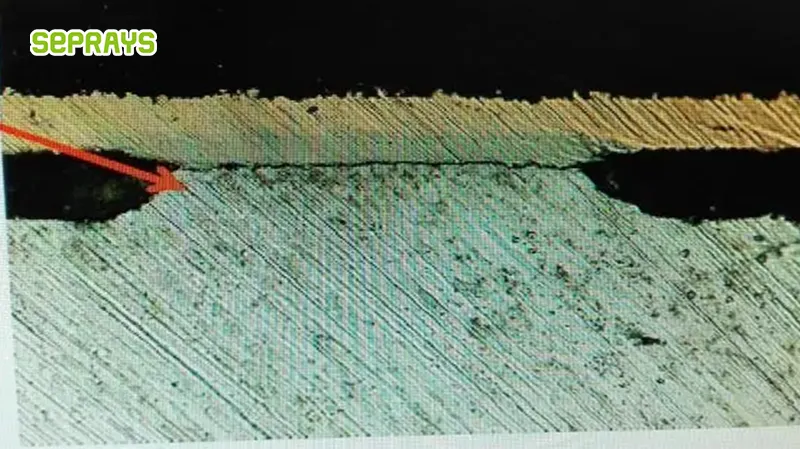
The challenge is that stress damage is often invisible at first.
Micro-cracks may only appear later during:
- vibration testing
- thermal cycling
- transportation
- long-term field use
This is why some failures seem “random” even when the SMT process itself looks stable.
⚠️ Why High-Density PCBA Is More Sensitive in 2026
PCB layouts today are dramatically different from older designs.
Many boards now include:
- ultra-fine pitch ICs
- edge-mounted connectors
- stacked components
- thinner substrates
- rigid-flex structures
That leaves less tolerance for mechanical force.
Even slight board bending during depaneling can damage solder joints under BGA or QFN packages.
One surprising reality:
The highest risk is often not visible damage.
It is hidden internal stress.
This is why some manufacturers now evaluate depaneling processes before finalizing PCB layouts.
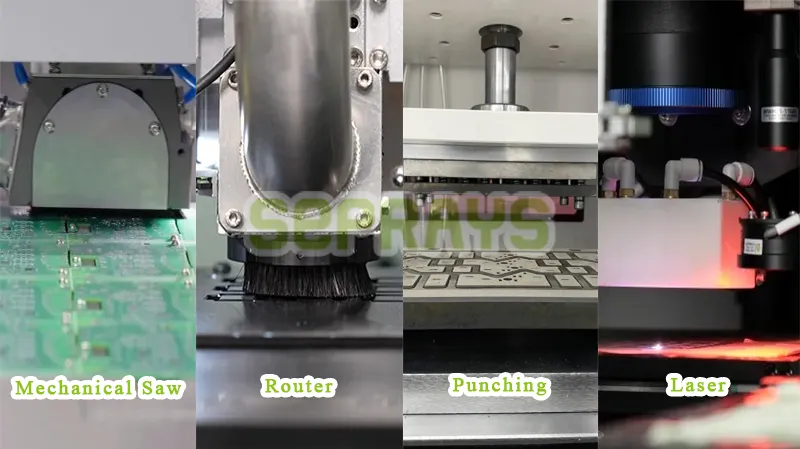
🛠️ Depaneling Method Matters More Than Many Realize
Different depaneling methods create very different stress levels.
Stress comparison by method:
| Depaneling Method | Stress Level | Typical Application |
|---|---|---|
| Manual breaking | High | Low-cost simple boards |
| Punch depaneling | Medium to high | High-volume fixed shapes |
| V-groove saw | 中 | Straight-line panels |
| ルーター depaneling | Low | Complex PCBA |
| レーザー depaneling | Very low | Sensitive high-density boards |
A common mistake is choosing the fastest method without considering board sensitivity.
That may reduce short-term production cost… but increase long-term failure risk.
📉 The Hidden Cost of Excessive PCB Stress
Factories usually notice PCB stress indirectly.
Typical symptoms include:
- intermittent electrical failures
- solder joint cracking
- connector instability
- increased rework
- field returns
- inconsistent ICT results
These issues are expensive because troubleshooting takes time.
Sometimes, engineering teams spend weeks analyzing SMT parameters before discovering that the actual issue came from depaneling stress.
Hidden production costs:
| Problem | Business Impact |
|---|---|
| Rework increase | Higher labor cost |
| Yield reduction | Lower throughput |
| Reliability failures | Warranty risk |
| Production downtime | Delivery delays |
| Scrap boards | Material waste |
In automotive electronics, especially, one hidden crack can become a major quality issue later.
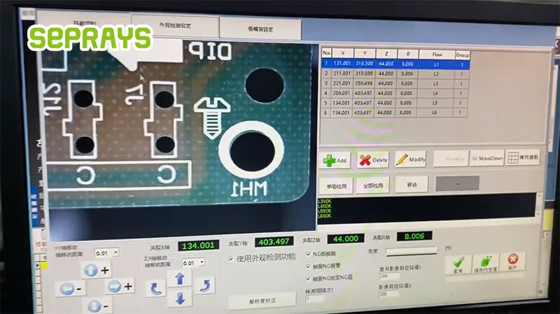
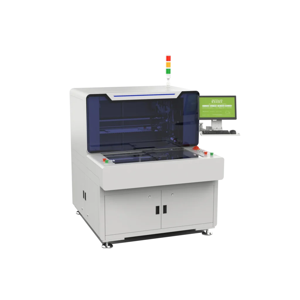
🚀 Why CCD Vision Systems Help Reduce Stress
Modern CCD vision systems are not only about positioning accuracy.
They also help reduce unnecessary cutting force.
Benefits include:
- more accurate cutting paths
- reduced alignment error
- better component protection
- improved consistency
- lower mechanical vibration
This becomes important when components sit very close to board edges.
In high-mix production, CCD systems also reduce setup variation between batches.
That helps maintain stable production quality.
🧩 Real Factory Scenario: Automotive BMS Production
A manufacturer producing EV battery management boards faced recurring reliability issues after vibration testing.
Initial investigations focused on:
- solder paste
- reflow profiles
- component quality
But the real issue was PCB stress generated during depaneling.
Their original process used manual V-cut separation because it was fast and inexpensive.
However, the boards contained:
- edge-mounted connectors
- dense BGA layouts
- multilayer structures
After working with Seprays engineers, they upgraded to:
- low-stress router depaneling
- CCD alignment
- customized support fixtures
- optimized routing paths
The interesting result:
Defect reduction was noticeable even before SMT parameter optimization.
That surprised the production team.
🔧 Practical Ways to Reduce PCB Stress
Several process improvements can significantly lower stress levels.
Recommended approaches:
- Use low-stress depaneling methods
- Improve board support fixtures
- Reduce unnecessary manual handling
- Maintain sharp routing tools
- Optimize cutting speed and feed rate
- Add CCD vision alignment
- Avoid excessive board bending
- Improve conveyor support consistency
Another important point:
Not every board needs laser depaneling.
Sometimes, optimized router processing provides the best balance between cost and stress control.
That depends on:
- board material
- PCB thickness
- edge clearance
- production volume
- reliability requirements
📊 Which Boards Need Extra Stress Protection?
Some PCB types are far more sensitive than others.
High-risk assemblies include:
| PCB Type | Why Stress Is Critical |
|---|---|
| Automotive BMS boards | Vibration reliability |
| ADAS modules | Dense layouts |
| Medical electronics | Long-term stability |
| Flexible PCB | Material softness |
| Rigid-flex boards | Structural complexity |
| Semiconductor PCBA | Precision requirements |
For these products, depaneling becomes part of reliability engineering.
Not just cutting.
🏭 Why Automation Helps Reduce PCB Stress
Automation reduces variability.
That matters more than many factories expect.
Fully automated systems improve:
- positioning consistency
- fixture stability
- handling precision
- cutting repeatability
Human handling differences disappear.
This is one reason more manufacturers are switching to automated depaneling systems in 2026.
Not only for speed.
But for process stability.
Ironically, slower and more controlled cutting sometimes improves total production efficiency because yield becomes more stable.
That sounds counterintuitive, but many high-reliability factories already follow this logic.
💡 The Future Trend: Stress-Aware Manufacturing
More manufacturers are now treating PCB stress as a measurable production factor.
Future trends include:
- inline stress monitoring
- AI-assisted cutting optimization
- smarter fixture design
- automated quality traceability
- hybrid low-stress depaneling systems
The conversation is changing.
Factories are no longer only asking:
“How fast can the machine run?”
They are asking:
“How reliably can we protect the board?”
That shift is important.
Why Choose Seprays Group?
With more than 30 years of experience in PCB/FPC depaneling technology, Seprays Group has supported manufacturers across automotive, semiconductor, communication, industrial control, medical electronics, and consumer electronics industries worldwide.
Seprays Group provides a complete range of depaneling solutions, including:
- milling-cutter depanelers
- レーザー depanelers
- V溝depanelers
- punching depanelers
- inline automation systems
- robotic handling solutions
Our equipment is trusted by internationally recognized manufacturers such as Foxconn, Flextronics, State Grid, Luxshare, Compal, Wistron, China Electronics, Quanta, CRRC, China Aerospace, OPPO, ZTE, and Bosch.
These systems are widely used in factories across China and global markets where production stability and PCB reliability are critical.
Beyond equipment supply, Seprays engineers help customers with:
- PCB stress analysis
- sample evaluation
- depaneling process optimization
- automation integration
- high-density PCBA solutions
- customized low-stress cutting recommendations
For manufacturers dealing with sensitive assemblies or complex SMT production requirements, choosing the right depaneling process can significantly improve long-term product reliability and yield.
If you are evaluating low-stress PCB depaneling solutions, please feel free to contact Seprays Group for technical discussion or sample testing.
WhatsApp: +8618929266433
Eメール: sales@seprays.com
FAQ
1. What causes PCB stress during depaneling?
PCB stress is mainly caused by vibration, bending force, improper support, aggressive cutting methods, and inconsistent handling during separation.
2. Which depaneling method creates the lowest PCB stress?
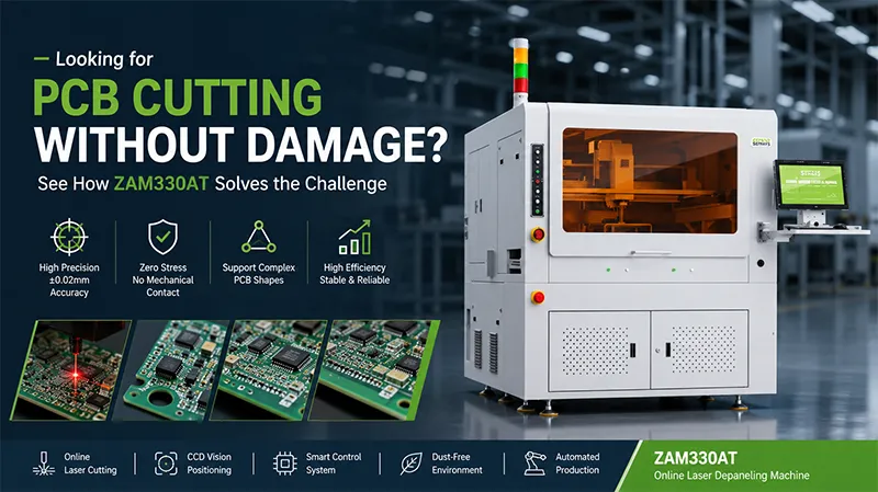
Laser depaneling generally produces the lowest mechanical stress, while precision router depaneling is also widely used for sensitive high-density PCBA.
3. Why are high-density assemblies more vulnerable to stress?
Components are placed closer together and near the PCB edges, leaving less tolerance for vibration, flexing, and mechanical forces.
4. Can PCB stress cause hidden failures?
Yes. Hidden micro-cracks and solder damage may only appear later during thermal cycling, vibration testing, or long-term product use.
5. How can manufacturers reduce PCB stress effectively?
Using low-stress depaneling methods, proper fixtures, CCD vision alignment, automated handling, and optimized process parameters can significantly reduce PCB stress risk.