.png)
 Japanese
  English
  Spanish
  Korean
  Russian
  Chinese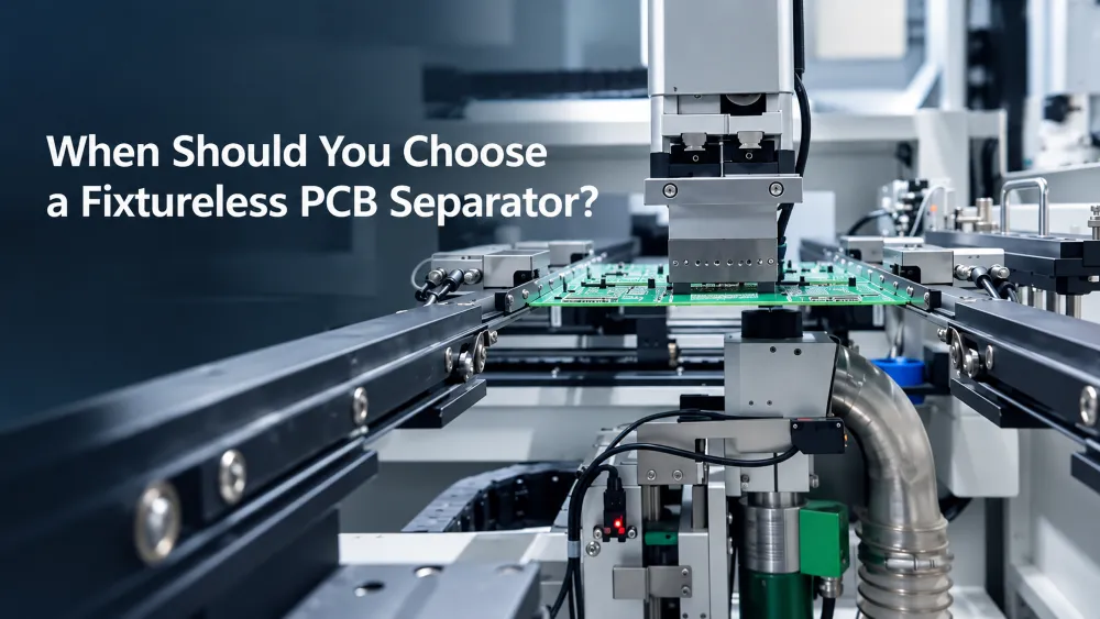
When Should You Choose a Fixtureless PCB Separator?
Fixtureless PCB separation sounds attractive when production teams are dealing with frequent PCB changes. No dedicated fixture to store. No fixture change every time the product changes. Less preparation before production. But there is a catch. A fixtureless process is not automatically the better choice. The real question is whether the PCB can be separated reliably without depending on a dedicated mechanical fixture. For some semiconductor and electronics manufacturers, that can save time and reduce recurring tooling costs. For others, a properly designed fixture still provides better support and repeatability. So when should you choose a fixtureless approach? 🏭 Start With the Production Problem Imagine a factory running eight PCB models during the same week. Model A runs in the morning. Model B runs after lunch. A small batch of Model C comes in the afternoon. Every change may require more than changing a machine program. If each PCB needs its own fixture, the operator may need to: None of these tasks actually separates a PCB. But they consume production time. This is where a fixtureless process becomes interesting. 🔍 What Does “Fixtureless” Really Mean? The term can be misunderstood. Fixtureless does not mean that the PCB has no positioning
PCB Routing in Action: A Real-World Depaneling Solution at a Customer Production Site
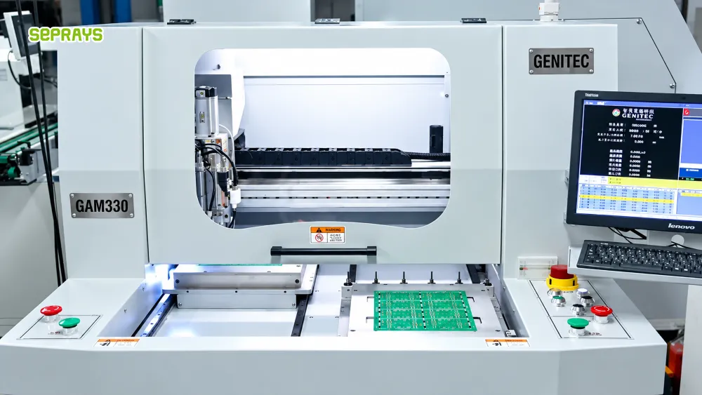
PCB routing sounds simple until it becomes part of a real production line. A semiconductor electronics manufacturer was facing a familiar problem: the PCB panels were changing, production volume was increasing, and manual separation was becoming harder to control. The team did not simply need a faster cutter. They needed a process that could load the panel, locate it correctly, follow the programmed contour, and separate the boards with consistent edge quality. This is where a GAM330 automatic PCB router machine from Seprays Group was evaluated for the production application. 🏭 Customer Production Challenge The customer manufactures electronic assemblies used in a semiconductor-related application. At first, the depaneling process looked manageable. But several small problems started adding up. Operators had to position panels manually. Different PCB models required repeated adjustments. Cutting consistency depended partly on operator experience. There was also another concern. The closer components move toward the PCB edge, the less room there is for uncontrolled mechanical stress, vibration, or an inaccurate cutting path. For production engineers, these issues are rarely isolated. A few seconds saved during cutting may mean little if operators spend extra time positioning panels or checking every separated board. So the customer started looking at
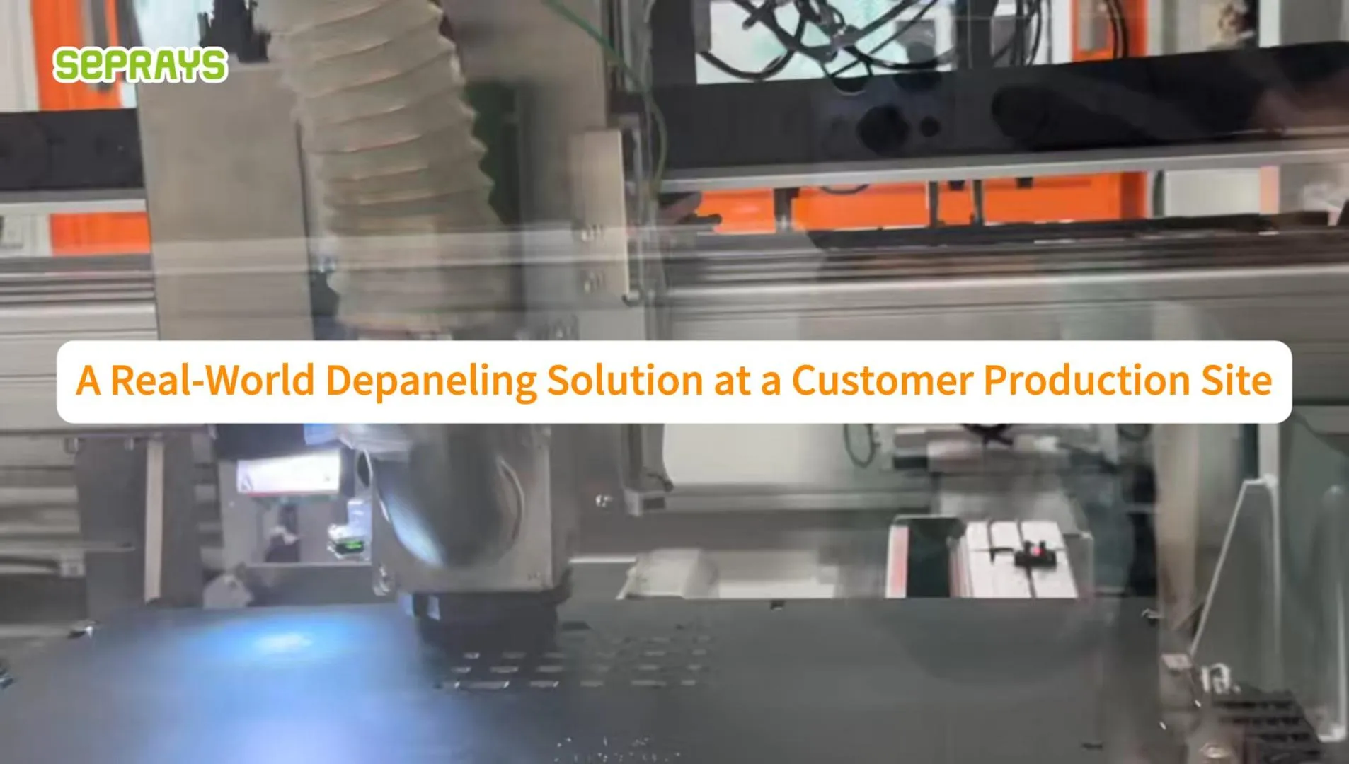
PCB Milling in Action: A Real-World Depaneling Solution at a Customer Production Site
PCB milling is not always the first process engineers think about when choosing a depaneling method. But on a real production line, the question is usually more practical: Can we separate the boards cleanly without damaging components, slowing production, or creating unnecessary costs? That question became particularly relevant at a semiconductor electronics manufacturing site where the production team was working with different PCB outlines, relatively high-value assemblies, and frequent product changes. Instead of looking for the fastest cutting method on paper, the team focused on something more useful: which process could remain stable when the PCB design changed? 🏭 The Production Problem Was More Than Just Cutting The customer was producing electronic assemblies for semiconductor-related equipment. The PCB panels were not all simple rectangles. Some included curves, irregular outlines, and routed tabs. Component density was also increasing around the board edges. The previous separation process created several practical concerns: This is where a programmable milling process became worth evaluating. A router-based process can follow different programmed contours without requiring a new die for every PCB design. That flexibility is one of its main advantages for high-mix production. ⚙️ What the Milling Process Looks Like on the Factory Floor The actual

Automated Laser PCB Depaneling for AI Hardware and High-Performance Electronics Manufacturing
Automated Laser PCB Depaneling becomes much more interesting when the PCB is no longer a simple board. AI servers, semiconductor equipment, automotive electronics, and high-performance computing systems often use boards with dense components, fine traces, unusual outlines, and tighter quality requirements. In these applications, the question is not simply, “How fast can we separate the panel?” A better question is: Can the separation process keep up with the board’s accuracy, quality, and automation requirements? That is where laser processing starts to make practical sense. 🔍 Why AI Hardware Changes the Depaneling Problem AI hardware is pushing electronics manufacturing toward higher component density and more complex PCB structures. A small amount of mechanical stress can become a quality concern when components are sensitive or when the board contains fine interconnections. Traditional mechanical cutting methods can still be highly effective for many applications. But they may not be the first choice when manufacturers need: For these applications, the cutting method needs to be considered together with the entire production process. ⚙️ What Makes Laser Processing Different? Laser cutting removes material without direct contact between a cutting tool and the PCB. That changes several things. There is no milling cutter gradually wearing against
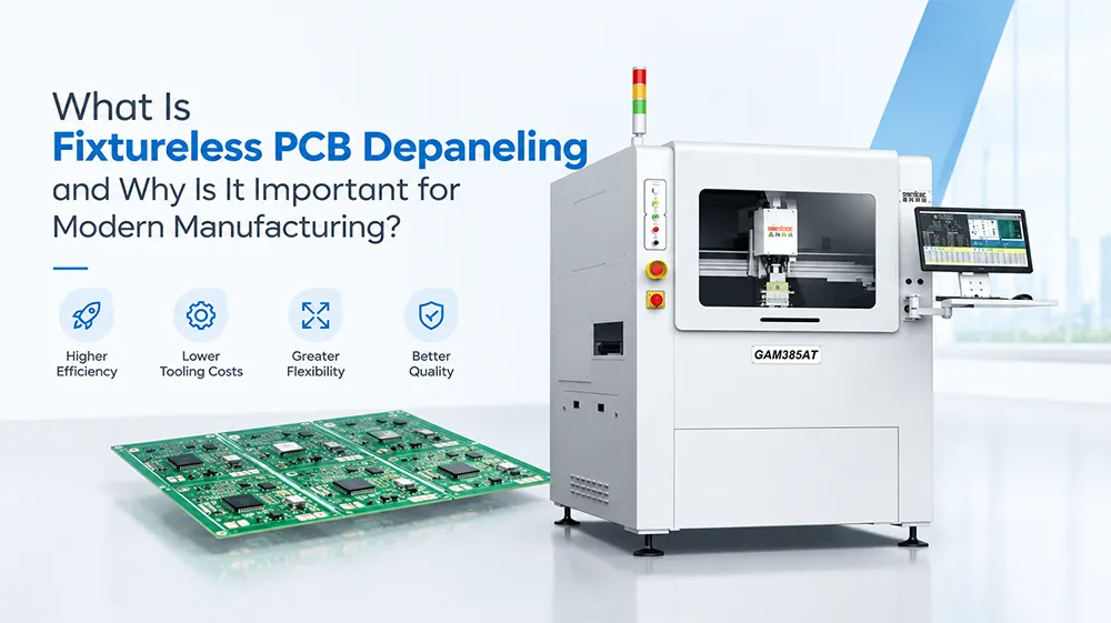
What Is Fixtureless PCB Depaneling and Why Is It Important for Modern Manufacturing?
Fixtureless PCB Depaneling is becoming an increasingly discussed topic among electronics manufacturers that need faster production, lower tooling costs, and more flexible PCB separation processes. For many factories, the challenge is not simply cutting a PCB panel. The real problem is how to maintain accuracy, protect sensitive components, and reduce downtime when product designs change frequently. Traditional depaneling methods often require dedicated fixtures for different PCB designs. This approach works well for stable mass production, but it can create additional costs when manufacturers handle multiple models, small batches, or frequent engineering changes. As electronics become smaller and more customized, many manufacturers are rethinking whether traditional fixture-based processes can still meet modern production requirements. 🔍 Why Traditional PCB Depaneling Creates Production Challenges In the early stages of electronics manufacturing, many factories produced a limited number of PCB models with long production cycles. Dedicated fixtures were practical because the investment could be recovered over millions of units. However, today’s manufacturing environment is different. Many companies face: A fixture designed for one PCB may become useless when the board shape changes. For example, an automotive electronics supplier may produce several control modules for different vehicle platforms. Each PCB requires slightly different positioning. Building
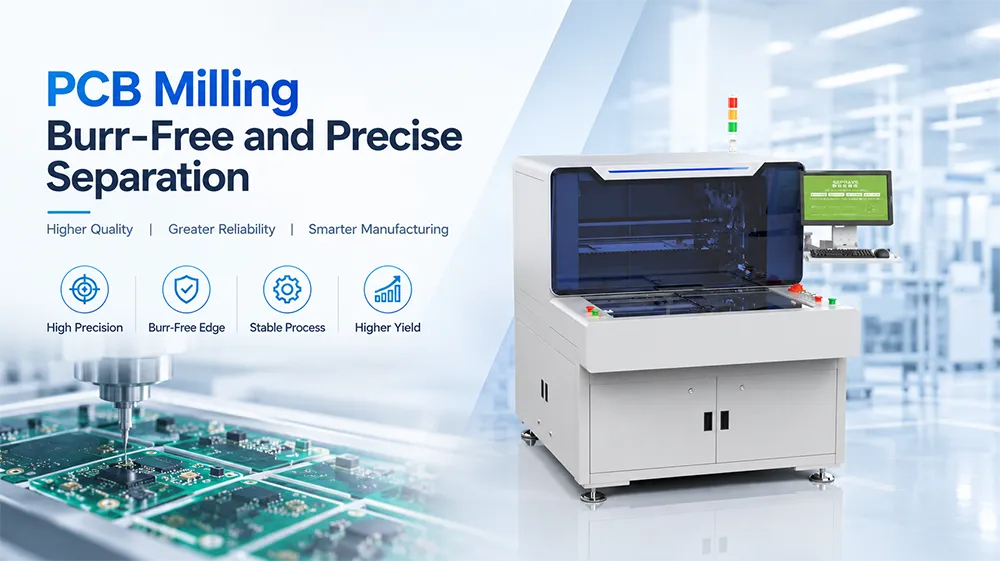
How PCB Milling Achieves Burr-Free and Precise PCB Separation
PCB milling sounds straightforward: a rotating cutter follows a programmed path and separates individual boards from a panel. In production, however, getting a clean edge is not simply a matter of increasing spindle speed. The real challenge is controlling cutting force, tool condition, positioning, support, dust, and board movement at the same time. A board can look acceptable after separation but still have small burrs, dimensional variation, lifted traces, or stress around sensitive components. These problems often become expensive later, especially when the PCB enters final assembly. So, what actually makes a milled PCB edge clean and repeatable? 🔍 Why Do Burrs Appear During PCB Separation? Burrs usually come from an unstable cutting process rather than a single machine setting. Common causes include: Tool wear deserves particular attention. As a cutter becomes dull, cutting resistance can increase. The result may be a rougher edge, more debris, dimensional variation, or even tool breakage. Tool condition and cutting parameters therefore need to be managed together rather than treated as separate issues. Practical lesson: a faster cutter does not automatically produce a cleaner PCB. ⚙️ How Does the Milling Process Stay Precise? A stable process normally depends on four factors working together. 1.