.png)
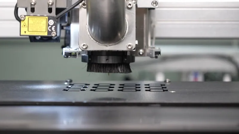
Will there be burrs after cutting the PCB with a milling cutter PCB depaneling machine?
Milling cutter PCB depaneling machine burr formation is one of the most common concerns raised by process engineers—especially when boards move directly into functional testing, coating, or final assembly. Burrs may look minor, but in high-density or high-reliability electronics, they can become a real quality risk. So, will burrs appear after milling and depaneling? The realistic answer is: they can—but they are controllable. This article shares production-level insights from EMS and OEM factories, focusing on industrial quality, durability, and practical process control rather than idealized claims. 🧠 What Engineers Mean by “Burrs” in PCB Depaneling In real production, burrs typically refer to: Not all burrs are equal. Some are cosmetic, […]
How Much More Efficient is a Dual-Platform Milling Cutter Depaneling Machine Compared to a Single-Platform One?
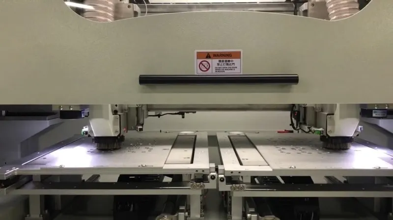
Dual-platform milling cutter depaneling machine efficiency is a topic that frequently arises when SMT lines encounter throughput bottlenecks, but hesitate to add headcount or floor space. On paper, the answer seems simple: dual platforms mean higher output. In reality, the efficiency gain depends on workflow design, product mix, and how “productive time” is defined on the shop floor. This article shares practical observations from EMS and OEM factories, focusing on industrial quality, durability, and realistic return on investment—rather than idealized cycle-time calculations. 🔍 Understanding the Real Bottleneck in Single-Platform Routing In many single-platform systems, the limiting factor is not cutting speed, but non-cutting time, such as: Field data shows that […]
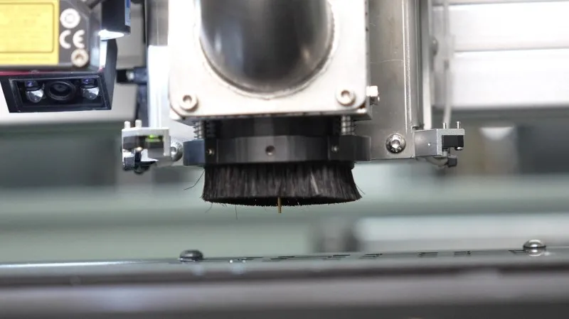
How Effective is the Dust Collection System of the Milling Cutter PCB Depaneling Machine?
Milling cutter PCB depaneling machine dust collection performance is often underestimated until production problems appear. Fine fiberglass dust, resin particles, and copper debris generated during routing do not just affect cleanliness—they directly influence yield, equipment lifespan, and operator safety. So how effective are modern dust collection systems in real SMT environments? This article shares practical, experience-based insights from global EMS and OEM production lines, focusing on industrial quality, durability, and long-term operational value rather than specifications alone. 🧠 Why Dust Control Matters More Than It Seems In high-density PCBA production, routing dust creates several hidden risks: Many engineers only notice dust issues after yield drops or maintenance intervals are shortened. […]
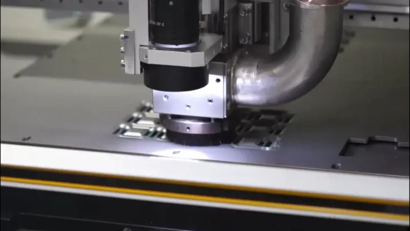
Can a Milling Cutter PCB Depaneling Machine Achieve a Cutting Accuracy of ±0.05 mm?
Milling cutter PCB depaneling machine accuracy is a recurring discussion point among process engineers working with high-value and high-density PCBAs. ±0.05 mm is often quoted in specifications—but can it be achieved consistently in real production? The short answer is yes, under defined conditions. The longer answer depends on process control, mechanical design, and expectations around repeatability versus peak performance. This article shares field-proven insights from EMS and OEM production lines, focusing on industrial quality, durability, and realistic cost–performance trade-offs. 🧭 What Does ±0.05 mm Accuracy Actually Mean in Production? In practice, cutting accuracy refers to the deviation between the programmed tool path and the final board edge. Engineers often discover […]
PCB Milling Depaneling Machine: Maintaining Edge Accuracy for High-Value PCBA

PCB Milling Depaneling Machine has become a cornerstone for high-value, high-density PCBAs where precision, edge integrity, and component safety are critical. Unlike V-cut or blade depaneling, milling provides controlled material removal and is especially effective for dense layouts, fragile boards, and applications demanding high reliability. This article explores practical strategies, common challenges, and field-tested solutions shared by engineers in global SMT environments. ⚙️ Understanding the Importance of Edge Accuracy For high-value PCBAs, edge accuracy is not just cosmetic—it affects: Even slight deviations or burr formation can result in micro-cracks, electrical shorts, or customer returns, highlighting the need for precise milling parameters and fixture support. 🧩 Challenge 1: Spindle Vibration and […]
Low-Stress Depaneling Solutions: Practical Approaches for Fragile and Dense PCBAs

Low-Stress Depaneling Solutions have become a priority as PCBAs grow thinner, denser, and more functionally integrated. In applications such as automotive electronics, industrial controls, and medical devices, depaneling is no longer viewed as a simple mechanical step—it is a process that can directly influence long-term reliability. This article shares practical approaches that engineers report actually working on fragile and high-density PCBAs. ⚙️ Why Fragile PCBAs React Differently to Depaneling Dense PCBAs often combine fine-pitch components, edge-mounted connectors, and multi-layer stackups. During depaneling, even moderate mechanical force can propagate stress into sensitive areas. Common pain points reported by SMT engineers include: Because these issues rarely appear during visual inspection, depaneling-related stress […]
PCB Depaneling Stress Reduction Techniques: What Actually Works in High-Density PCBA

PCB Depaneling Stress Reduction Techniques have become a crucial topic in high-density PCBA production. As boards become more compact, populated with sensitive components, and multi-layered, mechanical stress during depaneling can lead to micro-cracks, solder joint fatigue, and long-term reliability issues. This article presents field-tested approaches, practical fixes, and engineering insights from global SMT lines. ⚙️ Understanding Stress in High-Density PCBA Depaneling High-density PCBA presents unique stress challenges: Engineers report that even minor deviations in tool alignment or panel support can trigger latent defects, which often remain hidden until thermal cycling or vibration testing. 🧩 Technique 1: Optimized Router Parameters Routing remains a widely used depaneling method for dense boards. Key […]
PCB Depaneling for High-Density PCBA: Common Routing Challenges and Best Fixes

PCB Depaneling for High-Density PCBA has become a critical process as component spacing continues to shrink and functional integration increases. In modern SMT lines, routing is often the preferred depaneling method for dense layouts, but real-world production reveals recurring challenges that can affect yield, reliability, and long-term stability. This article summarizes practical lessons and proven fixes shared by engineers across global manufacturing sites. ⚙️ Why High-Density PCBA Is Especially Sensitive to Routing High-density PCBAs typically feature fine-pitch components, edge-mounted connectors, and multi-layer structures. During routing, even minor vibration or tool wear can transfer stress into solder joints or ceramic components. Engineers frequently report: These issues often pass visual inspection but […]
FPC Depaneling Solutions for Industrial Electronics: Field-Tested Strategies for Yield Stability

FPC Depaneling Solutions for Industrial Electronics are gaining attention as flexible circuits become more common in control systems, power modules, sensors, and human–machine interfaces. Compared with rigid PCBs, FPCs introduce unique challenges during depaneling due to their thin substrates, mixed materials, and sensitivity to mechanical stress. This article shares field-tested insights from industrial SMT environments focused on yield stability rather than short-term throughput. 🧠 Why FPC Depaneling Is a Yield-Sensitive Process Industrial electronics often operate in harsh conditions, making early-stage process stability critical. Engineers report that FPC-related yield loss frequently originates not in assembly, but during panel separation. Common challenges include: Unlike rigid boards, FPC defects may not be immediately […]
How to Reduce Mechanical Stress in PCB Depaneling

How to Reduce Mechanical Stress in PCB Depaneling has become a critical discussion in modern SMT production. As PCBs become thinner, denser, and populated with sensitive components, uncontrolled mechanical stress during separation can lead to micro-cracks, solder joint fatigue, and reduced reliability over time. This article shares insights from global SMT lines on minimizing stress, balancing cost, and improving yield. ⚙️ Understanding Mechanical Stress in Depaneling Mechanical stress arises whenever a PCB is separated from its panel using routers, V-cut, or blade depaneling systems. Common stress points include: Engineers emphasize that stress is not always visible at AOI but can manifest later during thermal cycling or vibration tests, especially in […]

