.png)

PCB Vカット分板の仕組み
基板のVカットdepaneling is a simple but clever manufacturing technique that helps separate multiple circuit boards from a single panel. First, precise V-shaped grooves are cut along the dividing lines on both sides of the panel, leaving just a thin connecting layer of material in the middle, much like perforations on a sheet of stamps. When it’s time to separate the boards, workers or machines can easily snap them apart along these pre-cut grooves. This method is fast, cost-effective, and works especially well for rectangular boards with straight edges.
メーカーが慎重に制御する深さのカットをクリーンの休憩を傷つけずに部品、一般的に出して、基板の厚さをカット. ながらV-切断に使用できない複雑な曲面形状は非常に脆弱な基板で一つの大量生産標準Pcbす。 のプロセスは強度が必要なの製造に簡単に分離時の基板をご用意しています。
標準的なVカット設計パラメータ
Vカット角度
● Typical Angle: 30°–45° (most common: 30°).
● Purpose: Balances ease of breaking with structural integrity during panel handling.
残存厚さ(アンカット層)
● Standard: 1/3 of the total board thickness (e.g., for a 1.6mm PCB, each side is cut ~0.5mm deep, leaving ~0.6mm uncut in the middle).
● Minimum: 0.3mm (to prevent accidental breakage during handling).
● Maximum: 0.8mm (beyond this, manual breaking becomes difficult).
Vカット幅(溝口)
● Standard: 0.2mm–0.5mm (depends on cutter tool size).
● Tighter Tolerance: ±0.1mm (for high-precision designs).
距離からの部品
● Minimum Clearance: ≥3mm from components/pads (per IPC-7351).
● Critical Areas: ≥5mm from BGA, fine-pitch ICs, or impedance-controlled traces.
パネルの強度を考慮
● Stress Relief Holes: Add 1.0mm–1.2mm holes at V-Cut ends to prevent cracking.
● Avoid Thin Boards: Not recommended for PCBs < 0.8mm thick (risk of warping/breaking).
公差基準
● Cut Position Accuracy: ±0.15mm (Class 2 IPC standard).
● Depth Consistency: ±0.05mm (critical for automated depaneling).
Vカット分板の適用例
単板形状
● Perfect for straight-line breaks (rectangles, squares);
● Ideal when all boards in the panel are the same size.
標準厚板
● Works best for 0.8mm to 3.0mm thick rigid PCBs;
● Most common for 1.6 mm-thick consumer electronics boards.
コスト面を考慮した事業
● 3-5x cheaper than routing for large batches;
● Faster production (can process thousands of panels per hour).
大量生産
● Excellent for mass production of simple designs;
● Minimal tooling changes are needed between jobs.
スペース効率の高いデザイン
● Allows tighter panel packing than routing (boards can be closer together);
● Leaves more usable panel space than tab routing.
SEPRAYS社のPCB Vカット分板ソリューション
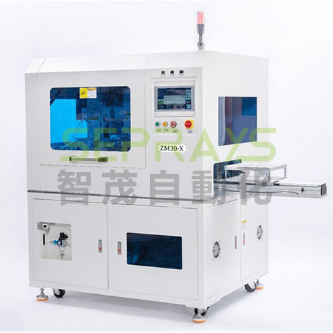
ZM30 PCB円刃Vカット分板機
The SEPRAYS’ ZM30 Round Knife PCB Separator is designed for various PCB circuit boards with V-grooves, including aluminum substrates, LED circuit boards, and LED light strips. Electronics manufacturers widely use it in the LED, SMT, mobile phone, toy, and other industries for efficient and precise board separation.

ZM30-X 自動V溝デパネラー
The machine offers advanced depaneling capabilities, featuring bidirectional (X/Y axis) automatic V-cut separation for precise panel division. It handles a wide range of materials with exceptional quality, including aluminum substrates (300-1500mm length), copper-clad boards, FR4, and fiberglass laminates – delivering smooth, burr-free cuts across all materials.
結論
Vカットdepanelingでありながらも、強力な解決を迅速に作り多くの回路です。 なにぴったりの状況での最適な選択肢はほとんどのための基本となる重要な事項のデザインです。 企業様SEPRAYS特殊機械の切り出した板を高速に行えますす。 どこより電子デバイス、スマート切断方法は今後も支援の工場で作業の高速化とスマート. かんのLED電話部品、理解Vカットでの生産は順調に進んでいます。