.png)
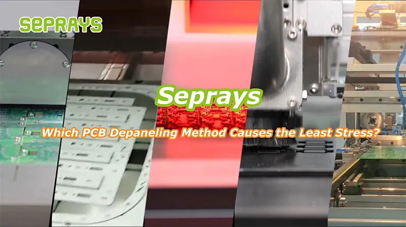
Which PCB depaneling method causes the least stress? For engineers and production managers, this question often arises when dealing with sensitive PCBs. In SMT manufacturing, edge cracks, micro-stress, and component damage can lead to rework, delays, and higher costs. Choosing the right depaneling technique is critical to maintain quality and throughput.
🔧 Understanding Stress in PCB Depaneling
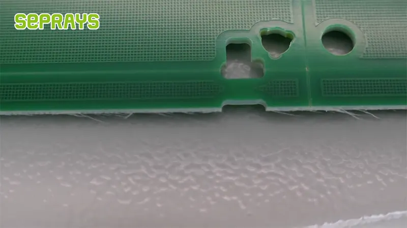
Stress in depaneling arises from mechanical force, vibration, or heat. Methods like sawing and punching physically push the board, which can:
- Crack brittle materials
- Strain edge-mounted components
- Introduce micro-fractures in solder joints
Reducing these stresses is essential for fragile, high-density, or multi-layer PCBs.
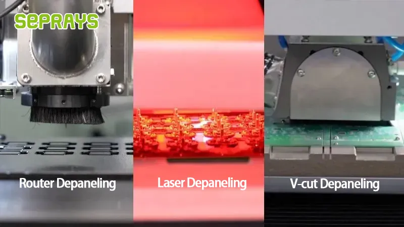
⚡ Comparing Common Depaneling Methods
Not all methods affect boards the same way. Here’s a practical overview:
| Method | Stress Level | Best Use Case | 速度 | Cost | Notes |
|---|---|---|---|---|---|
| Saw Blade | 中 | Straight-line V-groove boards | High | Low | Fast but can cause mechanical stress on edges |
| Router / Milling | 低-中 | Complex shapes | 中 | 中 | Cleaner edges, less vibration, suitable for irregular designs |
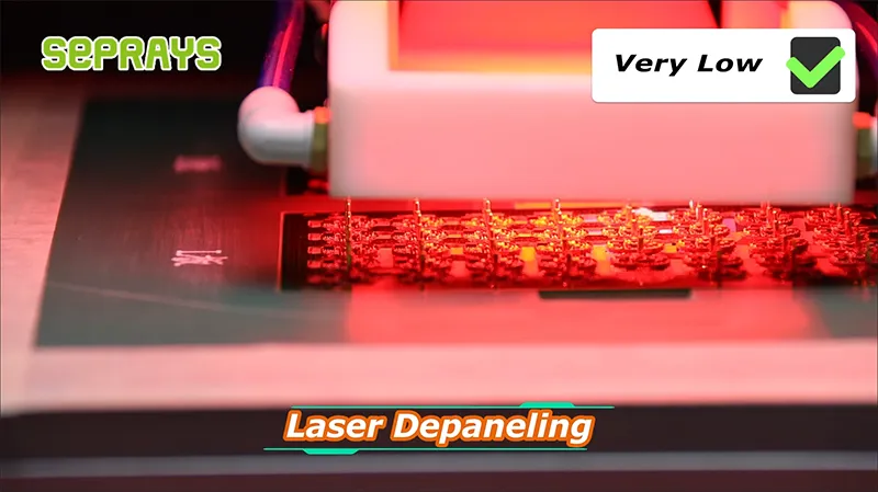
| レーザー Depaneling | Very Low | Sensitive, thin, high-density PCBs | 中 | High | Non-contact, minimal stress, excellent for delicate components |
| Punching / Stamping | 中 | High-volume standard boards | Very High | Low | Quick but mechanical impact can stress solder joints |
| V-Groove Breakout | Low | Straight-line boards | 中 | Low | Controlled snapping, low mechanical stress if properly designed |
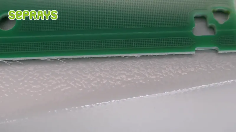
From this comparison, it’s clear that レーザー depaneling and properly executed V-groove breakout cause the least stress.
🧩 Why Stress Reduction Matters
Mechanical stress doesn’t always cause visible damage immediately. Common consequences include:
- Cracks forming during assembly
- Delamination of layers
- Reduced the lifespan of high-frequency boards
In mass SMT production, even minor stress translates into higher rework costs and lower yield.
🚀 Real-World Case: Sensitive PCB Manufacturing
A manufacturer producing multi-layer medical device boards faced repeated edge cracking during depaneling.
Challenges included:
- Ultra-thin layers
- High component density near edges
- Tight production schedules
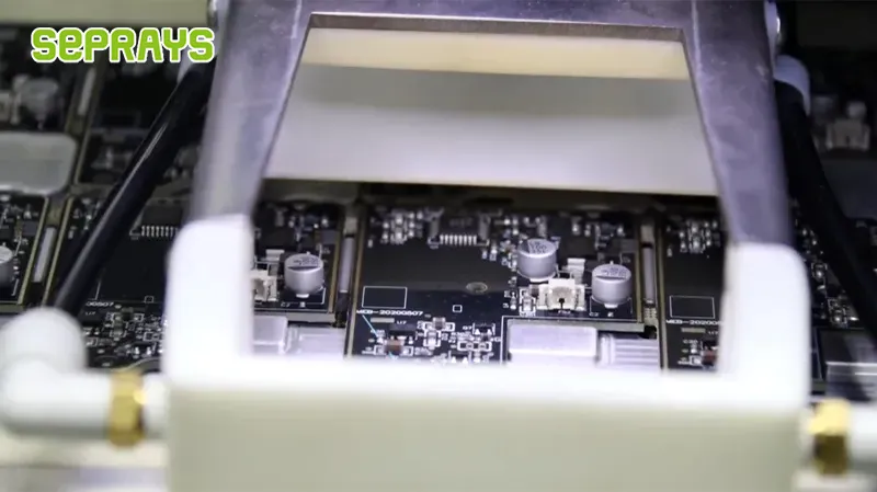
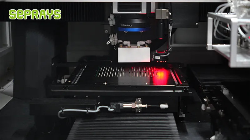
They worked with Seprays to implement レーザー depaneling. Results:
- Edge micro-cracks reduced by 90%
- Production speed is maintained with inline integration
- Operators required minimal additional training
The case highlights that selecting a low-stress method prevents defects without compromising throughput.
💰 Cost vs. Stress — Finding the Balance
While low-stress methods like lasers are more expensive upfront, they often reduce:
- Rework and scrap costs
- Assembly line failures
- Warranty claims
A simple ROI analysis often shows that investing in low-stress depaneling yields high-value, high-density PCB production.
| Factor | Saw Blade | Router | Laser | V-Groove | Punching |
|---|---|---|---|---|---|
| Equipment Cost | Low | 中 | High | Low | Low |
| Yield Impact | 中 | Low | Very Low | Low | 中 |
| Maintenance | Low | 中 | Low | Low | 中 |
| スループット | High | 中 | 中 | 中 | Very High |
This helps engineers weigh cost versus product quality when selecting a method.
🔄 Practical Tips for Minimizing Stress
Even within the same method, stress can be managed:
- Laser: Adjust power and speed to match board thickness
- V-Groove: Ensure proper scoring and controlled snapping
- Router: Optimize feed rate and spindle RPM
- Saw Blade: Use the correct blade thickness and stable fixtures
Small parameter tweaks significantly improve quality.
🛠️ When to Choose Each Low-Stress Method
- Laser depaneling: Best for ultra-thin or fragile PCBs, high-density SMT boards
- V-Groove breakout: Cost-effective for straight-line boards with moderate component density
- Router: Flexible for irregular or complex PCB shapes where stress must be minimized
Selecting the right method depends on PCB design, production volume, and sensitivity requirements.
🚀 Why Choose Seprays Group?
Seprays Group has been dedicated to PCB/FPC depaneling technology, providing a full range of solutions — milling cutter depanelers, laser depanelers, V-groove depanelers, punching depanelers, and automated handling systems.
Their equipment is trusted by leading manufacturers, including Foxconn, Flextronics, State Grid, Luxshare, Compal, Wistron, China Electronics, Quanta, CRRC, China Aerospace, OPPO, ZTE, and Bosch, serving factories across China and worldwide.
Seprays focuses on matching the right depaneling method to each production requirement, balancing cost, throughput, and stress reduction. Their solutions help manufacturers maintain high yield, improve reliability, and avoid costly defects.
If you need guidance on stress-free depaneling solutions, feel free to contact us.
WhatsApp: +8618929266433
Eメール: sales@seprays.com
❓ FAQ
1. Which method causes the least stress on PCBs?
Laser depaneling and V-groove breakout are generally the least stressful methods.
2. Can saw blade depaneling be used for fragile boards?
It can be, but it introduces more mechanical stress than laser or V-groove methods.
3. Does reducing stress affect production speed?
Advanced systems, such as lasers, maintain throughput while minimizing stress.
4. How can router depaneling minimize stress?
By adjusting the feed rate and spindle speed and using proper fixtures, stress is reduced.
5. Which method is best for high-density SMT boards?
Laser depaneling is preferred for its non-contact, low-stress operation.