.png)
 Japanese
  English
  Spanish
  Korean
  Russian
  Chinese
 Best Low-Stress PCB Depaneling Methods for Sensitive PCBA
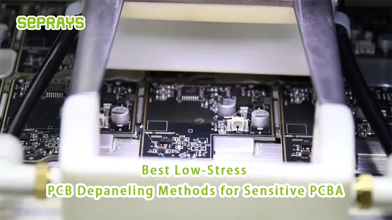
Best low-stress PCB depaneling methods for sensitive PCBA are becoming one of the most discussed topics in electronics manufacturing in 2026. Not because depaneling is new.But because PCB assemblies are getting more delicate every year. Smaller components.Thinner boards.Higher-density layouts. And less tolerance for stress. A process that worked five years ago may now create hidden reliability risks. 🔍 Why Sensitive PCBA Requires Low-Stress Depaneling Modern PCBAs often contain: These components are vulnerable to: The challenge is that damage is not always visible immediately. Sometimes failures appear only after: ⚙️ What Happens When Stress Is Too High? In real SMT production lines, common issues include: 1. Micro-Cracks in Solder Joints Especially […]
なぜ低ストレスが重要になるので基板Depaneling?
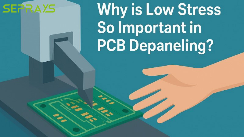
🛠 Low stress in PCB depaneling is critical for maintaining product quality and improving manufacturing efficiency. During the separation of individual boards from a panel, excessive mechanical stress can damage components and reduce overall yield. Understanding why low stress matters helps manufacturers choose the right depaneling solution for sensitive electronics. ⚙ What is Low-Stress PCB Depaneling? Low-stress PCB depaneling refers to separating printed circuit boards while minimizing mechanical forces that could affect the board or components. Modern depaneling machines, such as milling cutter depanelers, use precise cutting technology to reduce vibrations and prevent micro-cracks in solder joints. Key goals include: 💎 Protecting Components from Damage High stress during depaneling can […]