.png)
Why laser PCB depaneling is growing in modern electronics manufacturing is something many engineers are noticing on the shop floor. It’s not a trend driven by marketing. It’s driven by real production pressure—smaller devices, tighter layouts, and higher reliability requirements.
In the past, mechanical depaneling worked well enough.
Today, “good enough” is no longer enough.
🔍 What’s Changing in Electronics Manufacturing
Modern electronics are evolving fast.
Key shifts include:
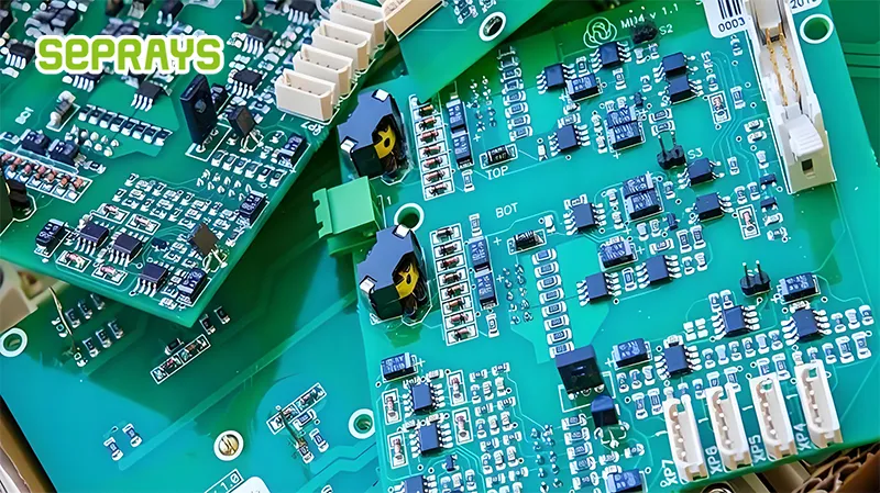
- Higher component density
- Thinner and more complex PCBs
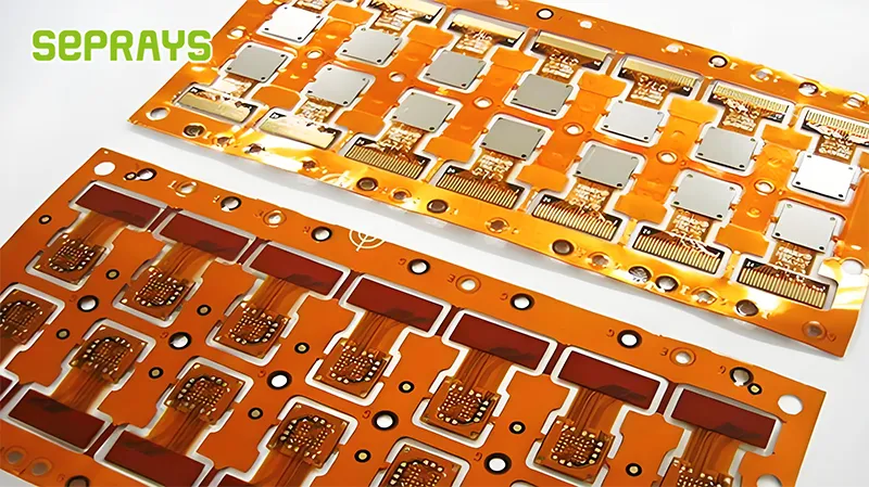
- Increased use of flex and rigid-flex designs
- Stricter reliability standards
These changes expose the limits of traditional depaneling methods.
What used to be a minor step is now a critical process.
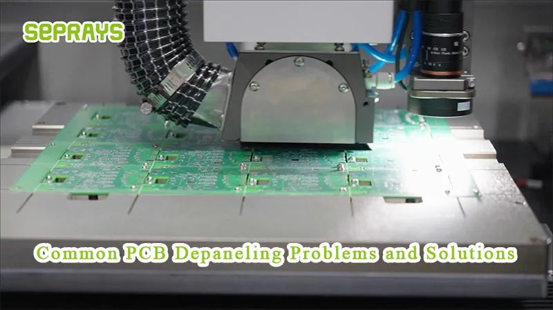
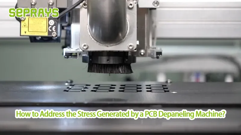
⚙️ The Limits of Mechanical Depaneling
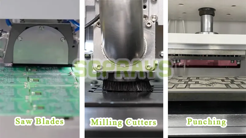
Mechanical methods—such as router, saw, and punching—are still widely used.
But they come with challenges:
- Mechanical stress on components
- Vibration affecting solder joints
- Tool wear leading to inconsistent quality
- Dust and debris contamination
For simple boards, these issues are manageable.
For high-density PCBs, they become a risk.
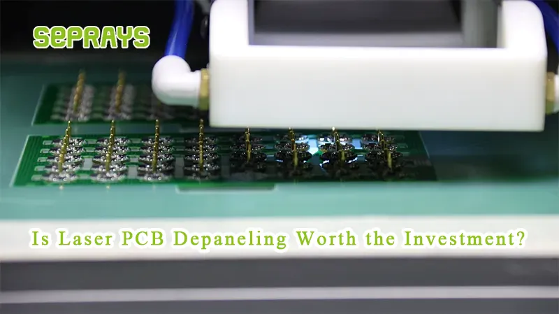
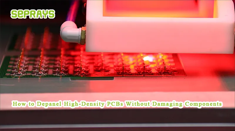
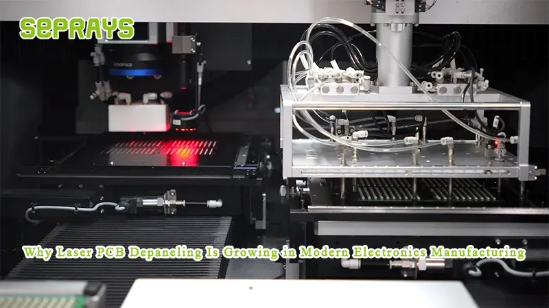
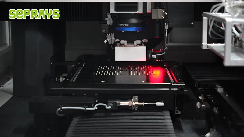
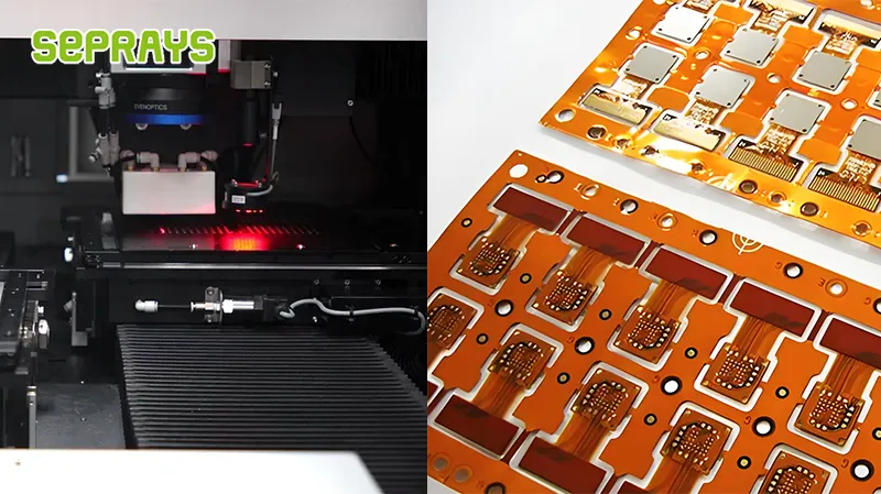
⚡ Why Laser Depaneling Is Gaining Ground
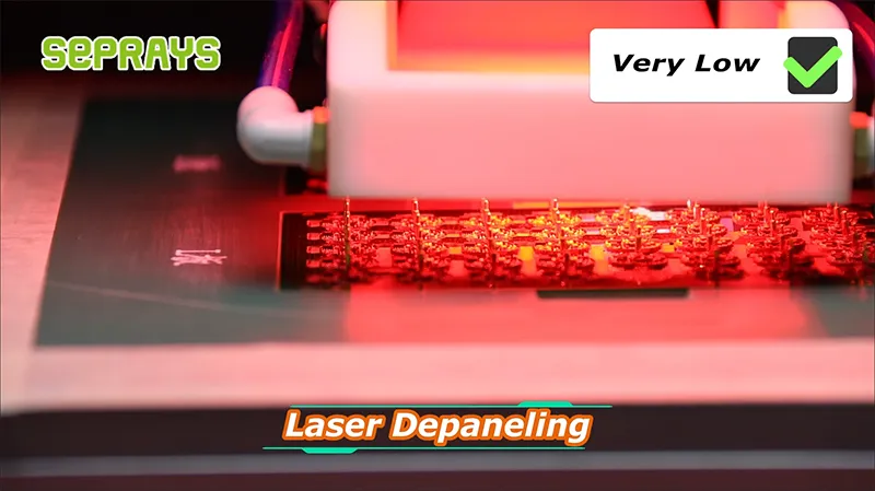
Laser PCB depaneling offers a different approach.
No contact.
No physical force.
This results in:
- Minimal stress on components
- High precision cutting
- Clean edges without burrs
- Better suitability for miniaturized designs
As PCB complexity increases, these advantages become more valuable.

📊 Laser vs Mechanical — A Practical Comparison
| Factor | Mechanical Methods | レーザー Depaneling |
|---|---|---|
| スプリント基板 | Medium to High | Very Low |
| 精密 | Moderate to High | Very High |
| ツールの摩耗 | あり | No |
| Dust Generation | High | Low |
| Suitability | Standard PCBs | High-density, flex PCBs |
The difference is not just technical.
It directly affects yield and reliability.
💥 Real Pain Points Driving the Shift
From real production feedback:
- Increasing failure rates after depaneling
- Components placed closer to edges
- Higher rework and inspection costs
- Inconsistent results across batches
These issues push manufacturers to rethink their processes.
Laser depaneling becomes a practical solution—not just an upgrade.
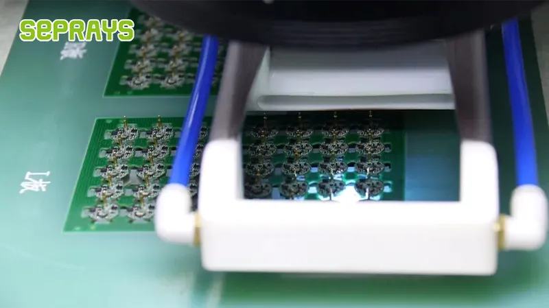
🧩 Case Study — Transition to Laser Depaneling
A manufacturer producing smart wearable devices faced recurring issues:
- Edge deformation on flexible PCBs
- Cracked components near cutting lines
- Rising defect rates
They collaborated with Seprays to implement レーザー depaneling.
Actions taken:
- Introduced laser cutting for sensitive boards
- Optimized parameters for material types
- Integrated with the existing SMT workflow
Results:
- Improved edge quality
- Reduced component damage
- More consistent yield
The transition was gradual.
But the impact was clear.
💰 Cost Perspective — More Than Equipment Price
Laser systems require a higher initial investment.
But the total cost includes:
- Scrap reduction
- Lower rework
- Improved reliability
- Reduced downtime
When viewed this way, laser depaneling often delivers long-term value.
Especially in high-volume production.
🔄 Where Laser Depaneling Fits Best
Laser PCB depaneling is most effective when:
- Working with high-density layouts
- Handling flexible or rigid-flex PCBs
- Components are near the board edges
- Product reliability is critical
For simpler designs, mechanical methods still have a place.
The key is choosing based on the application.
🛠️ Practical Considerations Before Switching
Before adopting laser depaneling:
- Evaluate PCB design and material
- Analyze current defect sources
- Consider hybrid solutions (laser + router)
- Plan integration with existing production lines
A balanced approach often works best.
🚀 The Future of PCB Depaneling
As electronics continue to evolve:
- Devices will become smaller
- Designs will become denser
- Quality expectations will rise
Laser depaneling is not replacing all methods.
But it is becoming essential in advanced manufacturing.
🚀 Why Choose Seprays Group?
Seprays Group focuses on delivering practical depaneling solutions for modern electronics manufacturing challenges.
Seprays Group has been dedicated to PCB/FPC depaneling technology, providing a full range of solutions — including milling cutter depanelers, laser depanelers, V-groove depanelers, punching depanelers, and automated handling systems.
Their equipment is trusted by leading global manufacturers such as Foxconn, Flextronics, State Grid, Luxshare, Compal, Wistron, China Electronics, Quanta, CRRC, China Aerospace, OPPO, ZTE, and Bosch. These partnerships reflect proven performance across high-density, flexible, and large-scale production environments.
With strong application experience, Seprays helps manufacturers transition to more advanced depaneling methods while maintaining efficiency and cost control.
If you are exploring laser depaneling for your production, feel free to contact us.
WhatsApp: +8618929266433
Eメール: sales@seprays.com
❓ FAQ
1. Why is laser depaneling becoming more popular?
Because modern PCBs are more complex and require low-stress, high-precision cutting.
2. Is laser depaneling suitable for all PCBs?
Not all. It is best for high-density, flexible, or sensitive boards.
3. Does laser depaneling improve yield?
Yes. It reduces defects caused by mechanical stress.
4. Is the investment in laser equipment justified?
For high-value production, the long-term savings often justify the cost.
5. Can laser and mechanical methods be combined?
Yes. Many manufacturers use hybrid approaches for optimal results.