.png)
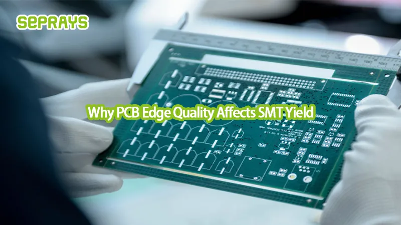
PCB edge quality is often ignored until production problems start showing up on the SMT line.
Boards pass AOI.
Placement accuracy looks normal.
Reflow profiles are stable.
But yield still drops.
In many factories, the real issue is not the solder paste or the placement machine. It is the PCB edge itself.
Poor depaneling quality can create burrs, stress cracks, edge deformation, and hidden micro-damage that directly affect SMT yield. As PCB designs become thinner and more compact in 2026, this issue is becoming harder to ignore.
Especially in:
- automotive electronics
- BMS systems
- communication modules
- medical electronics
- semiconductor-related PCBA
- flexible and rigid-flex boards
Many engineers are now paying closer attention to how panels are separated — not just how fast.
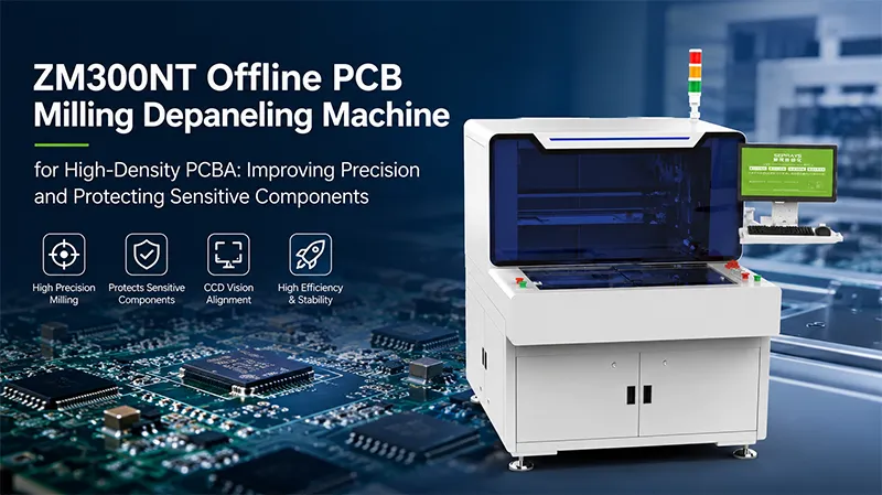
🔍 What Does “PCB Edge Quality” Really Mean?
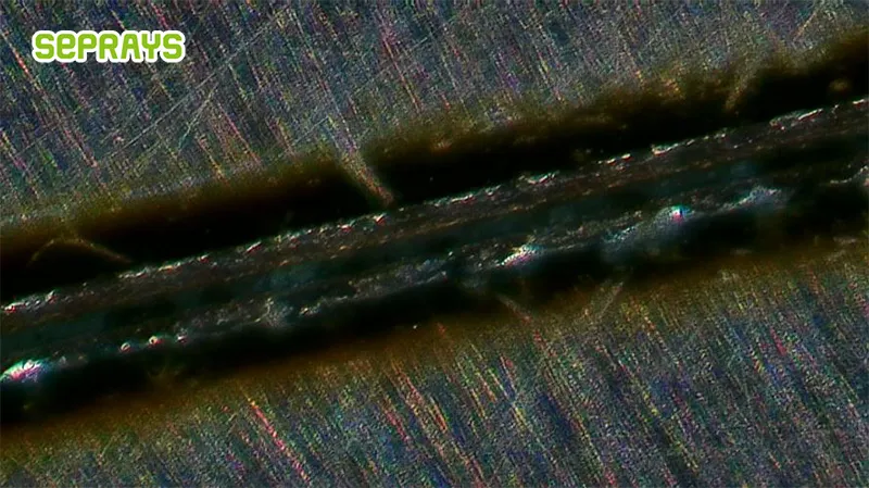
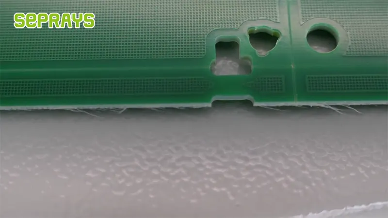
PCB edge quality refers to the condition of the board edge after depaneling.
It includes:
- burr level
- smoothness
- carbonization
- mechanical stress
- edge cracking
- delamination
- copper exposure
- debris contamination
A board may look “acceptable” visually but still carry microscopic stress damage.
That hidden damage can later appear as:
- Solder joint failure
- Intermittent electrical problems
- Component shifting
- Reduced reliability during vibration testing
This is especially critical for automotive and industrial electronics.
⚠️ Why Poor PCB Edges Reduce SMT Yield
Many SMT factories first notice the problem indirectly.
Typical symptoms include:
- rising rework rates
- unstable ICT results
- random functional failures
- inconsistent solder joints near board edges
- increased scrap during final assembly
The difficult part is that these issues often appear several processes later.
That makes troubleshooting harder.
Common edge-related production risks:
| Edge Problem | SMT Impact |
|---|---|
| Burrs | Component interference |
| Mechanical stress | Cracked solder joints |
| PCB warpage | Placement deviation |
| Dust contamination | Soldering defects |
| Edge cracking | Reliability failure |
| Delamination | Electrical instability |
Ironically, some factories upgrade SMT equipment first… while the actual issue comes from depaneling quality.
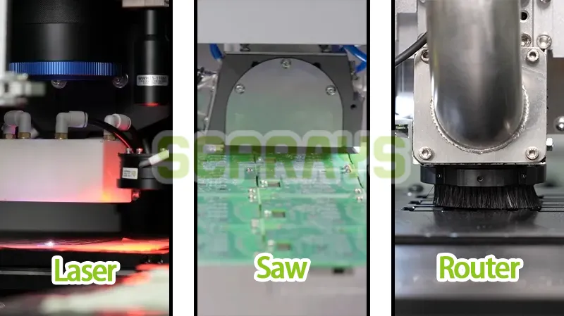
🛠️ The Connection Between Depaneling Method and Yield
Different depaneling methods create different levels of stress.
That matters more today because:
- Components sit closer to the edges
- PCB thickness continues shrinking
- Multilayer structures are more fragile
- Panel utilization is tighter
General stress comparison:
| Depaneling Method | Stress Level | Typical Use |
|---|---|---|
| Manual breaking | High | Low-cost simple boards |
| V-cut saw | 中 | Straight-line production |
| ルーター depaneling | Low | Complex PCBA |
| レーザー depaneling | Very low | High-density sensitive boards |
There is no “perfect” method for every board.
That is an important reality many purchasing teams miss.
The best process depends on:
- board material
- component spacing
- panel design
- production volume
- reliability requirements
🧩 A Common 2026 Problem: Components Too Close to the Edge
In 2026, compact electronic products will continue driving PCB miniaturization.
Design teams push components closer to board edges to save space.
That creates a new challenge for depaneling.
A cutting process that worked five years ago may now generate excessive stress.
Typical high-risk boards include:
- ADAS modules
- EV power boards
- wearable electronics
- RF communication devices
- medical sensors
In these cases, even slight vibration can create hidden solder fractures.
One factory producing automotive radar modules found that yield problems were not caused by reflow temperatures at all.
The actual issue was edge vibration during depaneling.
After switching from manual V-cut separation to precision router depaneling with CCD alignment, defect rates dropped noticeably.
📉 The Hidden Cost of Poor Edge Quality
Factories often focus on the machine purchase price.
But edge quality affects long-term manufacturing cost more than many realize.
Hidden costs include:
- higher rework
- reduced first-pass yield
- customer returns
- reliability failures
- production downtime
- engineering troubleshooting time
One damaged PCB may only cost a few dollars.
But one field failure in automotive electronics can become far more expensive.
That is why many Tier 1 suppliers now evaluate depaneling quality earlier during process planning.
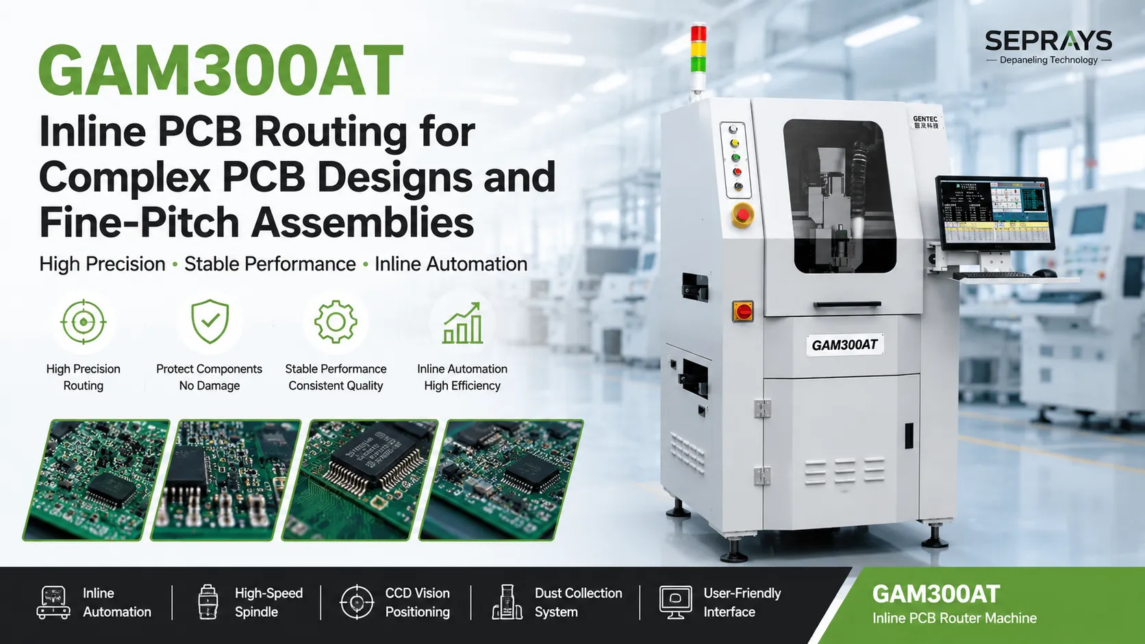
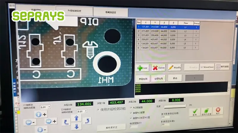
🚀 Why CCD Vision Systems Matter More Now
As PCB layouts become more complex, alignment accuracy becomes critical.
Modern CCD vision systems help:
- Compensate for panel tolerance
- Improve routing precision
- Reduce cutting deviation
- Protect nearby components
This is especially valuable for:
- irregular board shapes
- high-mix production
- flexible PCB
- rigid-flex assemblies
Interestingly, many engineers report that setup consistency improved more than cutting speed after adding vision systems.
That improves overall SMT stability.
🏭 Real Production Example from an Automotive Supplier
An automotive electronics manufacturer producing BMS control boards faced recurring edge defects during high-volume production.
Problems included:
- edge burrs
- connector stress
- inconsistent ICT results
Their previous depaneling setup used traditional saw separation.
After evaluating the process with Seprays engineers, they introduced:
- CCD-guided router depaneling
- vacuum dust extraction
- optimized support fixtures
- inline handling integration
The result was not only cleaner edges.
They also reduced operator intervention and improved overall SMT yield consistency during continuous production.
One lesson from the project stood out:
The cheapest depaneling process initially became the more expensive process later because of yield loss.
🔧 How Manufacturers Can Improve PCB Edge Quality
Several practical improvements can reduce edge-related defects.
Recommended approaches:
- Choose low-stress depaneling methods
- Optimize panel design early
- Maintain sharp cutting tools
- Reduce vibration during separation
- Improve dust extraction
- Use CCD alignment systems
- Test real boards before scaling production
Another important point:
Do not evaluate depaneling only by speed.
A slightly slower process with better edge quality may improve total factory efficiency.
That sounds counterintuitive, but many high-reliability manufacturers already follow this logic.
📊 Which Industries Care Most About PCB Edge Quality?
Some applications are far more sensitive than others.
High-priority industries include:
| 産業 | Why Edge Quality Matters |
|---|---|
| 自動車 | Vibration reliability |
| Medical | Long-term stability |
| Aerospace | High reliability standards |
| Semiconductor | Precision assembly |
| Industrial control | Continuous operation |
| Communication equipment | Dense PCB layouts |
For these industries, depaneling is not just a cutting process anymore.
It is part of quality control.
💡 The Future Trend in 2026
More manufacturers are now integrating depaneling decisions earlier in product development.
That shift is important.
Because once the PCB layout is finalized, solving edge stress problems becomes harder and more expensive.
Future trends include:
- smarter inline systems
- AI-assisted vision alignment
- lower-stress laser processing
- automated quality monitoring
- integrated MES traceability
Factories are no longer asking:
“How fast can this machine cut?”
They are asking:
“How stable is the final product quality?”
That is a very different conversation.
Why Choose Seprays Group?
With more than 30 years of experience in PCB/FPC depaneling technology, Seprays Group supports manufacturers facing increasingly demanding SMT and PCBA production challenges.
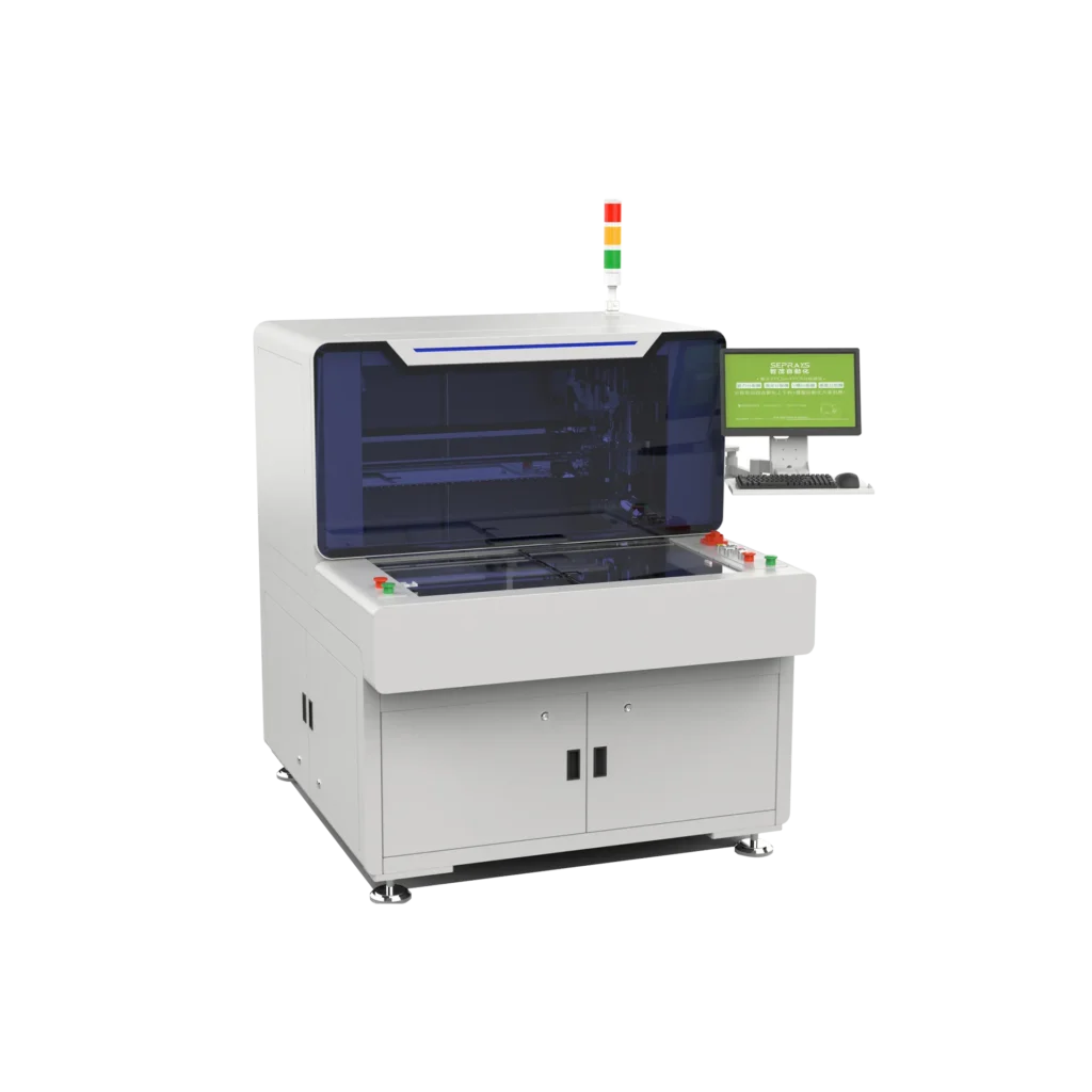
Seprays Group provides a full range of depaneling solutions, including:
- milling-cutter depanelers
- レーザー depanelers
- V溝depanelers
- punching depanelers
- inline automation systems
- robotic handling solutions
Our equipment is trusted by globally recognized manufacturers such as Foxconn, Flextronics, State Grid, Luxshare, Compal, Wistron, China Electronics, Quanta, CRRC, China Aerospace, OPPO, ZTE, and Bosch.
These systems are widely used in automotive electronics, semiconductor manufacturing, industrial control, communication devices, and medical electronics factories across China and worldwide.
What many customers value is not only equipment performance, but practical process support:
- stress evaluation
- sample testing
- inline integration
- customized depaneling recommendations
- high-density PCBA solutions
Seprays engineers work closely with manufacturers to help improve yield, reduce hidden production risks, and optimize long-term process stability.
If you are evaluating PCB depaneling solutions for sensitive or high-density PCBA production, please feel free to contact us for technical discussion or sample testing.
WhatsApp: +8618929266433
Eメール: sales@seprays.com
FAQ
1. Why does PCB edge quality affect SMT yield?
Poor PCB edges can create stress cracks, burrs, contamination, and warpage that affect soldering quality, component reliability, and final assembly consistency.
2. Which depaneling method produces the best PCB edge quality?
Laser depaneling generally provides the cleanest and lowest-stress edges, while router depaneling is widely used for balancing quality and production efficiency.
3. How can I reduce PCB stress during depaneling?
Using low-stress methods, CCD vision alignment, proper fixtures, sharp tools, and optimized cutting paths can significantly reduce PCB stress.
4. Are edge burrs really a serious production problem?
Yes. Burrs can interfere with connectors, create contamination, and increase the risk of assembly defects or long-term reliability failure.
5. Is router depaneling suitable for high-density PCBA?
Yes. Modern PCB router systems with CCD vision and precision motion control are widely used for high-density and sensitive electronic assemblies.