.png)

PCBレーザーデパネリングの分類
UVレーザーデパネリング
紫外線レーザー depaneling用紫外レーザーカット基板を高速かつ高精度で少します。 この方法は薄く、繊細な素材のようにフレキシブル回路基板(Fpc)、剛性フレックス。 で紫外線レーザーをクリーン、滑らかなエッジ損なうことなく、一般的に用いられるような業種医療機器の消費者エレクトロニクス、航空宇宙、細かいます。
CO₂レーザーデパネリング
CO₂レーザー depaneling用炭酸ガスレーザー切断剛性の基板材料などのFR4でいます。 これらの強力なレーザーカットできます早くも発熱量で少し焼いですね。 CO₂レーザーに最適用途軽炭化る場合がありますので使用を避けなどの産業エレクトロニクス、高出力デバイス
ファイバーレーザーデパネリング
ファイバーレーザー depanelingは主に切削加工で金属基板、アルミニウム又は銅板を設けました。 この作品を迅速-確実にでような業種LED照明、自動車、またはパワーエレクトロニクス しかし、ファイバレーザは一般的に使用のための標準基板材料FR4またはポリイミド.
PCBレーザーデパネリングの利点
高精度、クリーンカット
レーザー depaneling精度を確保し、バリ無しの切削のリスクを軽減損などのデリケートな基板ます。
無機械的ストレス
従来のルーティングやパンチング方法、レーザー depanelingは非接触プロセスをなく機械的ストレスに含まれております。
粉塵の低減
レーザー切断を最小限に粒子汚れに最適で要求される用途で高清潔さなど、医療や航空宇宙エレクトロニクス.
柔軟性のための複雑なデザイン
できる切削の複雑なパターンの微細レーザー depanelingに適した現代の基板設計を含め、不規則な形状の
さまざまな材料
ではFR4、ポリイミド(PI)、アルミニウム基板、その他の素材ですので汎用性を提供いたします。
最小限の熱放射能の影響を受けている地域(溶)
先端レーザーシステム制御放熱、熱損傷部品による高品質のドアップ。
生産効率の向上
高速自動運転に向スループット、レーザー depaneling、効率的なソリューションのための量産には向かない。
メンテナンスコストが低減され
とは異なり機械のツール耗、レーザーシステムの低消耗コストの比率も高まることが認められます。
の紫外線レーザー Depaneling
精密切削
紫外線レーザは簡単にカットしていく複雑な基板デザインです。
低熱の影響
生の少ない熱、火傷防止や被害に敏感な部品です。
滑らかなクリーンエッジ
Cuts without rough edges or dust improve the quality of the final product.
安全のために薄く、フレキシブル回路基板
作品やデリケートな素材がこすことなく、割れやストレスとなる。
材料の廃棄物
精密切削を保存材料や製造原価の低減。
工具摩耗
とは異なりブレード、レーザーな摩耗、メンテナンスコストの節減
作品の多くの基板の種類
ではFR4、ポリイミド、およびその他の共通の基板素材ですのに役立ちます。
のCO2レーザDepaneling
高速切削加工
CO₂レーザーカットを迅速に、高速化を実現します。
良い肉厚の厚い材料に
も厚い板のようにFR4でいます。
滑らかなエッジ
クリーンカットも熱マークが表示される場合があります。
物理的損傷
なので非接触方式ではな割れやストレスにしました。
カット形状
対応できる異なる基板の設計およびレイアウトです。
大量生産
高速-コスト-効果的な選択のための大規模なる。
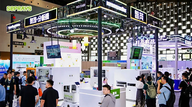
メSeprays'レーザー基板Depaneling機
- The automatic laser PCB separator adopts a compact design, which can save factory space.
- A variety of nanosecond and picosecond ultraviolet and green lasers are available for selection, capable of meeting various processing needs in the PCB industry.
- The entire series is equipped with a high-speed CCD vision automatic correction system, which can significantly improve cutting accuracy and operational efficiency.
- The fully automatic PCB separator handles the entire process from feeding and cutting to discharging, aligning with the requirements of automated factories.
- The processing area is fully enclosed, ensuring safety protection during the processing and complying with electrical standards in China and the European Union.
Seprays'レーザー基板Depaneling解
ZAM330ダブルプレーザー Depaneling機器
ZAM330 adopts a dual-table design, which saves the loading and unloading time, and keeps the laser always in the processing state. The processing area is 350mmx520mm, which is suitable for depaneling placed PCBs, open cover film window and other processes in SMT industry. Users can also equip the system with a camera target pre-positioning feature, which saves processing time by streamlining target positioning.

ZAM340インライン基板-レーザー Depaneling機器
ZAM340 takes the track inline processing, and the max working area can reach 350 x 350mm. The compact structure can quickly combine an SMT production line; therefore, it can be fit for any PCBA shaping. Users can easily switch between different types of production by using various tools and installing a 3-step track inline feeding system. On the other hand, conductive operation lets workers learn to use it quickly.

ZAM350シングルトレーザー Depaneling機器
ZAM350, the equipment using the classic bridge structure, uses an X/Y axis separation motion structure. The processing head moves on a stable bridge around the X direction, and the workpiece clamping platform moves along the Y axis back and forth. The two axes are independent and do not interfere with each other.

結論
レーザー depaneling の重要なツールに現代の基板製造、精密、速度や信頼性です。 からの紫外線レーザーのためのフレキシブル回路基板,CO₂レーザーの硬質材料、ファイバーレーザメタルコア基板の各メソッドは、独自の利益を代のニーズに合わせた生産ます。 無機械的ストレスが少ないため熱損傷に対処できる能力があるかを、複雑なデザインレーザー depaneling品質を向上させることが可能と対応の自動化にありがとうございます。 どのようにSeprays'レーザー depaneling機、プリント基板の製造を約束しても見ることができます。