.png)
GAM300AT Inline PCB Routing for Complex PCB Designs and Fine-Pitch Assemblies
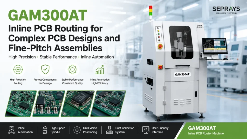
GAM300AT Inline PCB Routing is becoming a practical topic in manufacturing discussions because PCB designs are changing faster than many production processes can keep pace with. A few years ago, most boards followed relatively simple layouts with comfortable component spacing. Today, things look very different. High-density assemblies are becoming standard. Fine-pitch components continue shrinking. Board shapes are becoming more complex. And designers increasingly place components close to board edges. For production teams, this creates an uncomfortable reality: the assembly process may improve while depaneling becomes more difficult. Many factories only discover this after quality issues begin appearing. 🔍 Why Complex PCB Designs Create Unexpected Production Problems Traditional PCB layouts were […]
Looking for PCB Cutting Without Damage? See How ZAM330AT Solves the Challenge
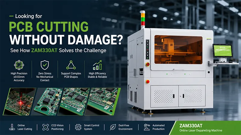
PCB cutting without damage has become a bigger discussion point in electronics manufacturing in 2026. Many production teams are discovering that achieving a clean separation is no longer enough. The board may look perfect after depaneling, pass visual inspection, and even complete electrical testing successfully—but hidden stress can remain inside the assembly. The problem is that damage is not always visible. Tiny micro-cracks, weakened solder joints, edge chipping, and invisible stress around sensitive components may not appear immediately. In some cases, failures only emerge after vibration testing, thermal cycling, or long-term field use. This creates an uncomfortable situation for manufacturers. Everything appears normal at first. Then, unexpected quality problems start […]
Happy Dragon Boat Festival: Warm Wishes from SEPRAYS · Genitec
Happy Dragon Boat Festival from SEPRAYS · Genitec! The Dragon Boat Festival is a meaningful tradition celebrated by many people around the world. It is a special time that brings together family, culture, and the spirit of unity. Through generations, this festival has carried values of perseverance, teamwork, and shared happiness, making it one of the most respected traditional celebrations. As we celebrate this special occasion, it is also a moment to appreciate the people around us—family members, friends, colleagues, customers, and partners who contribute to our daily lives and shared success. At SEPRAYS · Genitec, we would like to extend our sincere gratitude and best wishes to everyone celebrating […]
How to Depanel Mobile Phone Power Adapter PCBs Without Damaging Components – GAM330AT
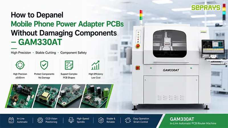
Mobile phone power adapter PCBs are getting smaller every year. Faster charging requirements, adoption of GaN technology, and more compact product designs are pushing components closer together than many manufacturers expected a few years ago. On paper, the design looks efficient. On the production floor, it often creates a different discussion. Engineers start noticing small but frustrating problems: Cracked solder joints. Damaged edge components. Micro-stress around sensitive ICs. Unexpected yield drops. And sometimes the depaneling process becomes the last place people investigate. The issue is that power adapter boards are no longer simple rectangular PCBs with large empty margins. In many cases, components sit only a few millimeters—or even less—from […]
Best PCB Routing Solutions for Complex Board Shapes
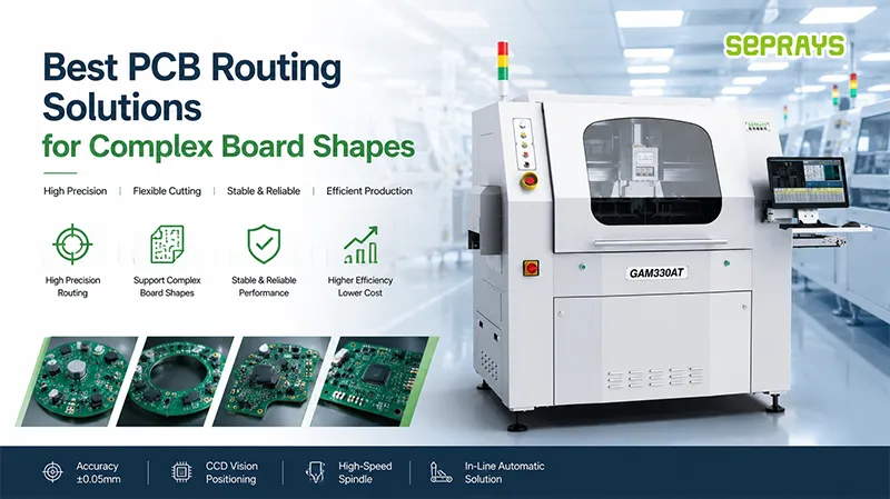
PCB routing solutions often become a serious discussion only after manufacturers run into problems. At the prototype stage, unusual board designs usually look manageable. But once production scales, irregular shapes start creating issues that are difficult to ignore. Rounded corners. L-shaped boards. Sensor modules with openings. Automotive control units with unique outlines. Wearable electronics with curved structures. On the screen, these designs look clean and efficient. On the factory floor, they can become a source of yield loss, longer cycle times, tool wear, and inconsistent separation quality. As product miniaturization continues in 2026, complex PCB geometries are becoming increasingly common across automotive electronics, industrial control systems, consumer devices, and IoT […]
Why Online PCB Separators Are Becoming Essential for Module Product Cutting in 2026

Online PCB Separators are no longer considered optional equipment in many electronics factories. In 2026, manufacturers of display modules, automotive sensors, communication modules, battery management systems, and smart electronic assemblies face a common challenge: increasing output while maintaining cutting-edge quality and reducing labor dependence. For years, many factories treated PCB depaneling as an isolated process. Boards were cut offline and transferred manually between workstations. Today, that approach is becoming a bottleneck. As module products become more complex and production lines become more automated, online PCB separation is increasingly viewed as a key part of smart manufacturing rather than just a cutting operation. 🔍 Why Module Product Cutting Has Become More […]
Three Key Changes Shaping the PCB Depaneling Industry After NEPCON 2026
The three-day NEPCON China 2026 has officially come to a close. As one of the most influential events in the electronics manufacturing industry, the exhibition brings together companies from consumer electronics, automotive electronics, new energy, medical devices, and many other sectors every year. For Seprays, attending the exhibition is about more than showcasing equipment. More importantly, it is an opportunity to listen to our customers. Throughout the event, we welcomed visitors from different countries and regions and had in-depth discussions with engineers, production managers, and business decision-makers. During these conversations, one thing became increasingly clear: The PCB depaneling industry is entering a new stage of transformation. Change 1: Customers Are […]
PCB Depaneling Automation: Why More SMT Factories Are Combining Routing and Unloading in 2026
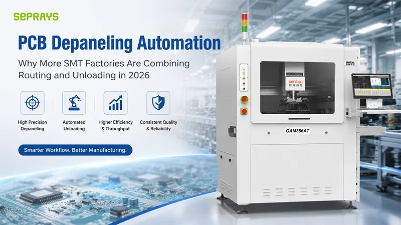
PCB depaneling automation is no longer just a topic discussed by large electronics manufacturers. Over the past two years, we have seen medium-sized EMS providers and OEM factories begin re-evaluating how much time, labor, and product risk still exist between the depaneling process and final board collection. Interestingly, many production managers focus heavily on cutting accuracy while overlooking what happens immediately after depaneling. In reality, manual board handling often creates hidden costs that are difficult to measure until production volumes increase. As labor costs continue rising in 2026 and manufacturers push for higher throughput, integrated depaneling and unloading systems are becoming a practical solution rather than a luxury investment. 🔍 […]
When Should You Use Laser PCB Cutting Instead of Routing?
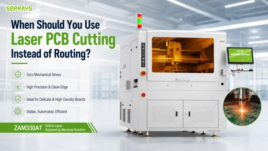
Laser PCB Cutting has become a topic of growing interest among electronics manufacturers in 2026. As PCB designs become smaller, denser, and more complex, many engineers are asking the same question: should they continue using traditional routing, or is laser technology now the better choice? The answer is not as simple as choosing the newest technology. In many production environments, routing remains highly effective. However, there are specific situations where laser depaneling can significantly improve product quality, yield, and long-term manufacturing efficiency. This article explores when laser cutting makes sense, where routing still excels, and how manufacturers can make a practical decision based on their actual production requirements. 🔍 Why […]
Best PCB Separation Solutions for EV and Automotive Electronics
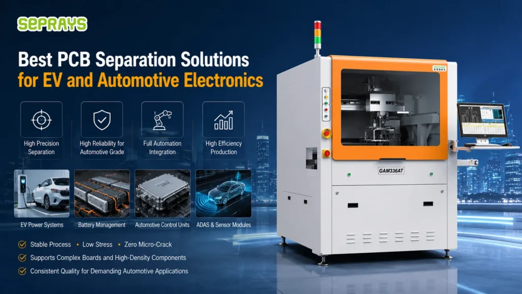
PCB Separation Solutions have become a critical part of EV and automotive electronics manufacturing. As vehicle electronics become more compact, intelligent, and safety-critical in 2026, manufacturers are paying much closer attention to what happens after SMT assembly. Many production teams focus heavily on soldering quality, AOI inspection, and testing. Yet an overlooked depaneling process can introduce hidden stress, micro-cracks, edge damage, or component failures that only appear later in the field. For automotive electronics, where reliability standards are far higher than those of consumer devices, choosing the right separation method is no longer just a production decision. It is a product quality decision. Let’s explore how manufacturers can select the […]

