.png)
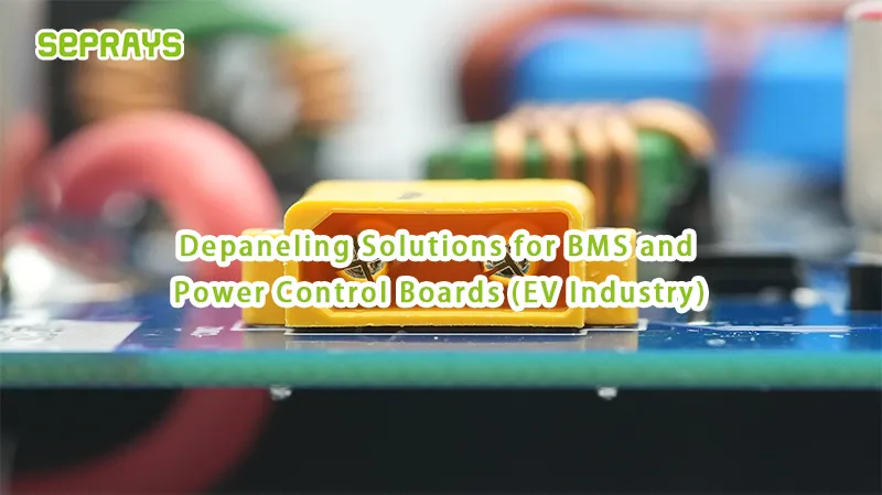
Depaneling solutions for BMS and power control boards are not just about separating PCBs. In EV manufacturing, they directly affect product safety, reliability, and long-term performance.
If you’ve worked with battery management systems or power control modules, you already know:
These boards are different.
Thicker. Heavier. More sensitive to stress.
🔍 What Makes BMS and Power Boards So Challenging?
From a user perspective, these PCBs typically have:
- Thick substrates (often >2.0mm)
- Heavy copper layers for high current
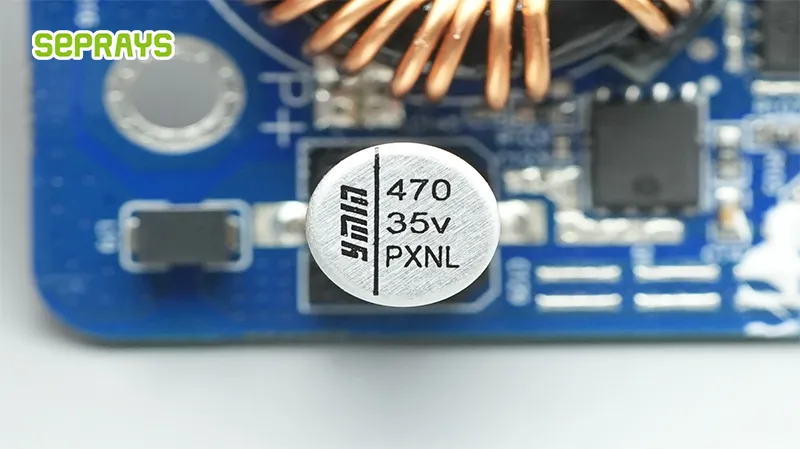
- Large components like capacitors and connectors
- Tight spacing in control areas
They are used in:
- Battery management systems (BMS)
- Inverters and converters
- Power distribution units
The challenge is simple:
You must separate the board without introducing mechanical or thermal damage.
⚙️ Why Standard Depaneling Methods Often Fail
Many factories initially use general-purpose methods.
But for EV boards, problems quickly appear:
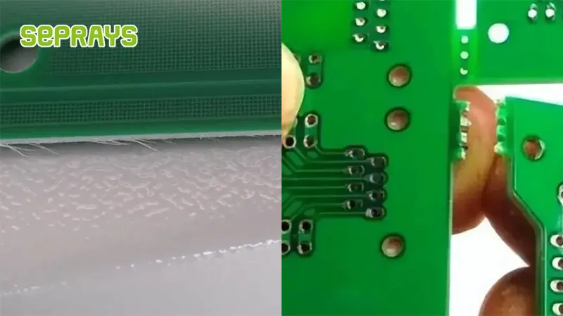
1. High Mechanical Stress
- Cracks in solder joints
- Damage to ceramic capacitors
- Hidden reliability risks
2. Poor Edge Quality
- Burrs on thick materials
- Delamination on multilayer boards
3. Low Efficiency
- Thick boards slow down routing
- Complex shapes increase cycle time
💥 Real Pain Points from Production Lines
Engineers working with EV electronics often report:
- “Boards pass inspection but fail in field testing.”
- “Depaneling becomes the bottleneck.”
- “High scrap cost due to edge damage.”
These are not random issues.
They are linked to the depaneling method.
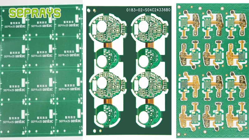
🧩 Which PCB Designs Need Specialized Solutions?
You likely need advanced depaneling if your boards include:
1. High-Current Power Paths
- Thick copper layers
- Heat-sensitive structures
2. Mixed Layout Areas
- Dense control circuits + large power components
- Different stress tolerance within one board
3. Complex Shapes
- Irregular outlines
- Multiple connection tabs
4. Automotive-Grade Requirements
- High reliability standards
- Strict quality consistency
💡 A Counterintuitive Insight
Many assume:
“Stronger boards can handle rough cutting.”
But in reality:
- Thicker boards store more stress
- Damage is harder to detect
- Failures appear later
Stronger structure ≠ Safer depaneling
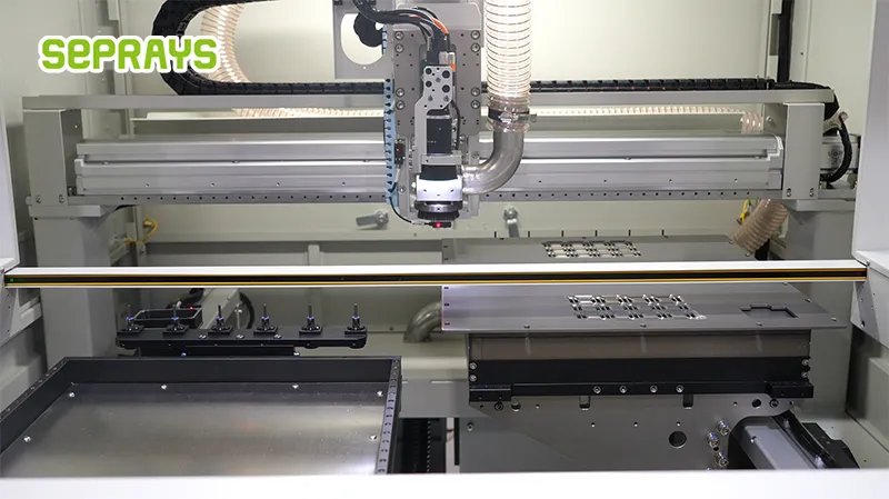
⚡ Best Depaneling Methods for EV Power Boards
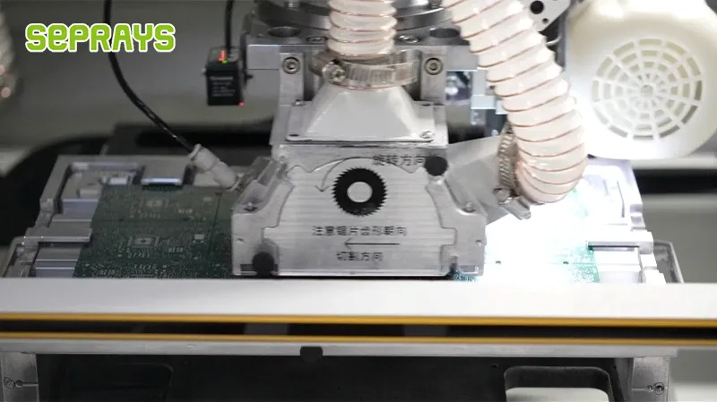
1. Router Depaneling
Best for:
- Thick boards
- Complex outlines
Advantages:
- Controlled cutting
- Good edge quality
Limitations:
- Slower for large panels
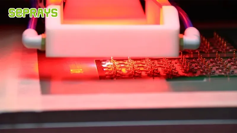
2. Laser Depaneling
Best for:
- Sensitive control areas
- Stress-free cutting requirements
Advantages:
- No mechanical stress
- High precision
Limitations:
- Higher cost
- Slower on thick materials
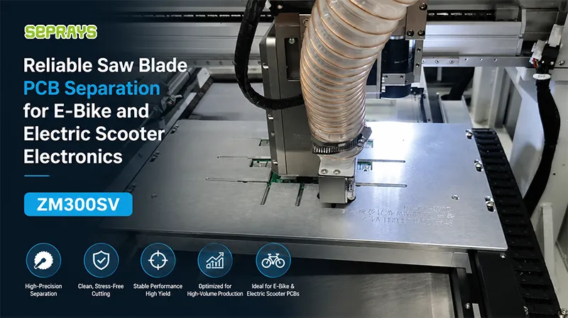
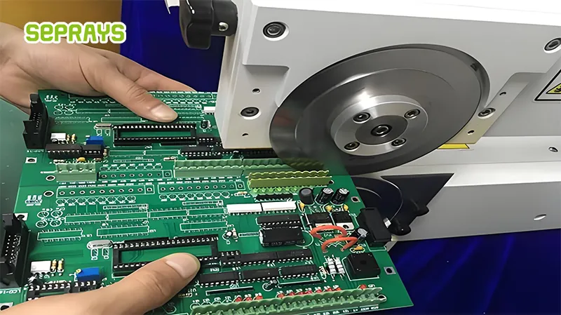
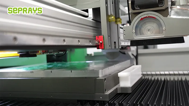
3. Saw Blade Depaneling
Best for:
- Straight-line cuts
- High-volume production
Advantages:
- 高速
- Efficient
Limitations:
- Mechanical stress risk
4. Hybrid Solutions
Best for:
- Mixed PCB structures
Advantages:
- Combine speed and precision
- Adapt to different board areas
📊 Method Comparison for BMS & Power Boards
| Method | Stress Level | 速度 | Thickness Handling | Best Use Case |
|---|---|---|---|---|
| Router | 中 | 中 | Excellent | Complex thick boards |
| Laser | Very Low | 中 | Limited | Sensitive areas |
| Saw Blade | Medium-High | High | Good | Straight cuts |
| Hybrid | Optimized | Optimized | Excellent | Mixed structures |
🧪 Case Example — EV Power Module Optimization
A manufacturer producing EV power control boards faced:
- Thick PCB panels (>2.5mm)
- High defect rate after depaneling
- Slow throughput using router-only solution
After working with Seprays, they adopted a hybrid approach:
- Router for complex contours
- Saw blade for straight sections
- Process optimization for stress control
Results:
- Reduced micro-cracks significantly
- Improved cutting speed
- Better production consistency
The key was not switching machines.
It was matching the method to each board section.
💰 Cost Considerations in EV Manufacturing
Depaneling cost is not just equipment cost.
It includes:
- Scrap and rework
- Reliability failures
- Production downtime
A cheaper method can become expensive if it causes defects.
In EV production, quality failures are far more costly than process upgrades.
🛠️ Practical Recommendations
From real-world experience:
- Test depaneling methods on actual EV boards
- Evaluate stress impact, not just cutting speed
- Use hybrid solutions for mixed designs
- Optimize parameters for thick materials
- Plan for future scalability
These steps reduce long-term risk.
🔄 When Should You Upgrade Your Depaneling Process?
Consider upgrading if:
- You are moving into EV or automotive production
- PCB thickness is increasing
- Defect rates are rising
- The current method limits efficiency
These are clear indicators.
🚀 Final Thought — Reliability Comes First
In EV electronics:
- Performance matters
- Safety matters more
Depaneling is a small step.
But it has a big impact.
🚀 Why Choose Seprays Group?
Seprays Group focuses on delivering reliable depaneling solutions for demanding industries such as EV and automotive electronics, helping manufacturers balance efficiency, quality, and long-term reliability.
Seprays Group has been dedicated to PCB/FPC depaneling technology, providing a full range of solutions—milling-cutter, laser, V-groove, and punching depanelers, as well as automated handling systems. Our equipment is trusted by leading manufacturers, including Foxconn, Flextronics, State Grid, Luxshare, Compal, Wistron, China Electronics, Quanta, CRRC, China Aerospace, OPPO, ZTE, and Bosch, and is used in factories across China and worldwide.
With extensive application experience, Seprays helps customers optimize depaneling strategies for EV boards, reduce defects, and ensure stable production performance.
If you are looking for the right depaneling solution for BMS or power control boards, feel free to contact us.
WhatsApp: +8618929266433
Eメール: sales@seprays.com
❓ FAQ
1. Why are BMS PCBs difficult to depanel?
Because they are thick, high-current, and stress-sensitive.
2. Is laser depaneling suitable for power boards?
あり, for sensitive areas, but less efficient for thick materials.
3. What is the best method overall?
Hybrid depaneling is often the most balanced solution.
4. Can the router handle thick PCBs?
Yes, it is one of the best methods for thick boards.
5. How to reduce depaneling defects in EV PCBs?
Use the right method, optimize parameters, and test with real production samples.