.png)
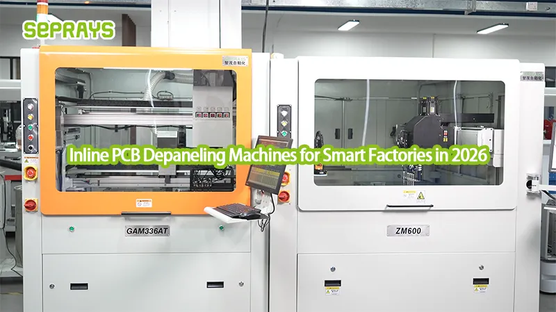
Inline PCB Depaneling Machines for Smart Factories in 2026
Inline PCB Depaneling Machines are becoming a serious topic inside modern SMT factories. Not because they look more advanced.Not because “Industry 4.0” sounds impressive. But because many production lines in 2026 are reaching a point where manual depaneling is becoming the bottleneck. A factory may already have: Yet the depaneling process still relies on operators to load and unload panels manually. That mismatch creates hidden inefficiencies. And as labor costs rise and product designs become more complex, more manufacturers are rethinking how depaneling fits into the entire production flow. 🔍 What Is an Inline PCB Depaneling Machine? An inline depaneling system connects directly with the SMT production line. Instead of separating boards offline at a separate workstation, the PCB moves automatically through the depaneling process as part of continuous production. Typical inline configurations include: In simple terms: The depaneling machine becomes part of the smart factory ecosystem rather than operating in isolation. ⚠️ Why Traditional Offline Depaneling Starts Creating Problems Offline systems still work well in many factories. Especially for: But in high-volume SMT environments, several problems appear over time. Common pain points: Interestingly, many factories do not notice these losses immediately. The SMT line still runs. Production still ships.
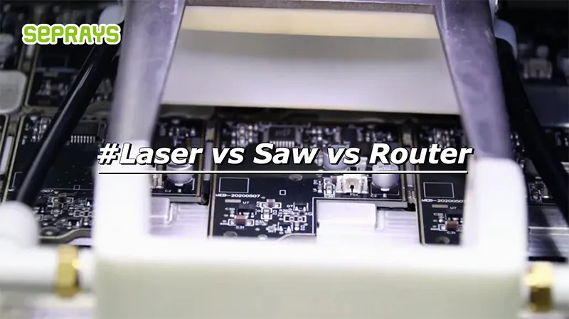
Laser vs Saw vs Router PCB Depaneling: Which Is Better in 2026?
Laser vs Saw vs Router PCB Depaneling is no longer just a technical comparison for process engineers. In 2026, it will directly affect: And here’s the interesting part: There is no single “best” depaneling method anymore. What works perfectly for consumer electronics may fail in automotive production.What saves cost in high-volume manufacturing may create problems in high-mix environments. That’s why more manufacturers are evaluating depaneling from a process perspective — not just machine specifications. 🔍 Why Choosing the Wrong Depaneling Method Gets Expensive Fast A surprising number of production issues start after SMT assembly. Not during soldering. Not during testing. But during depaneling. Factories often experience: The difficult part? These problems are sometimes blamed on PCB design or assembly quality. But the real issue may simply be the wrong depaneling process. ⚙️ Understanding the Three Main Depaneling Methods Before comparing performance, it helps to understand what each method actually does best. 🔹 Laser Depaneling Uses focused laser energy to separate PCB boards without physical contact. Best known for: 🔹 Saw Depaneling Uses high-speed circular blades for straight-line cutting. Best known for: 🔹 Router Depaneling Uses milling cutters to follow programmed cutting paths. Best known for: 📊 Laser vs Saw vs
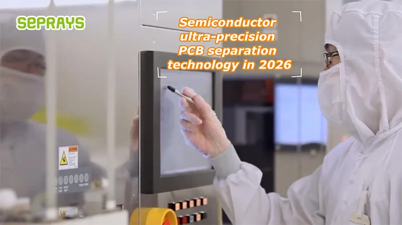
Why Semiconductor Manufacturers Need Ultra-Precision PCB Depaneling in 2026
Ultra-Precision PCB Depaneling is becoming a serious topic of discussion within semiconductor manufacturing facilities in 2026. Not because it sounds advanced.But because the margin for error is shrinking fast. A semiconductor customer once shared something surprisingly simple during a factory visit: “One tiny cutting deviation can ruin an entire high-value board.” That statement stayed with many engineers in the room. Today’s semiconductor PCBAs are: And the depaneling process — once considered a minor production step — is now directly tied to product reliability. 🔍 Why Semiconductor PCBAs Are More Difficult to Depanel Today Five years ago, many depaneling systems could tolerate small process variations. In 2026? Not anymore. Semiconductor-related PCBAs increasingly include: Some components are positioned extremely close to the board edge. That changes everything. Even minor vibration or cutting stress may lead to: The difficult part? Most defects are not immediately visible. ⚠️ The Hidden Cost of “Good Enough” Depaneling One common misconception is: “If the board looks fine after cutting, the process is acceptable.” But semiconductor manufacturing rarely works that way. A board can pass visual inspection while still containing: These problems may only appear later during: For semiconductor applications, delayed failure is often far more expensive than
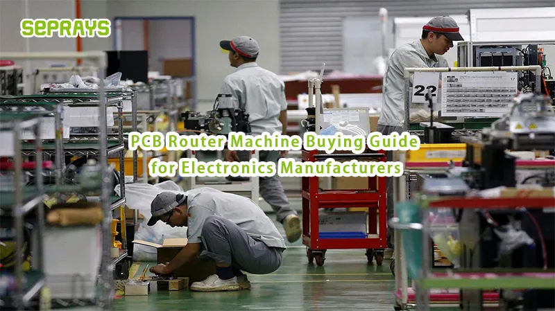
PCB Router Machine Buying Guide for Electronics Manufacturers
PCB Router Machine selection has become far more complicated in 2026 than many manufacturers expected. A few years ago, buyers mainly compared price and cutting speed.Today, the conversation is different. Factories now care about: And one important reality is often overlooked: The “best” router machine depends heavily on your PCB type, production model, and future expansion plans. A machine that performs well for consumer electronics may not fit automotive, medical, or industrial applications. 🔍 Why PCB Router Machines Still Matter in 2026 Despite the growth of laser depaneling, router depaneling remains one of the most widely used methods in electronics manufacturing. Why? Because it offers a practical balance between: Especially for: For many factories, router depaneling is still the most economical long-term solution. ⚠️ The Most Common Buying Mistake Many buyers focus only on machine specifications. But production problems usually come from process mismatch — not lack of machine power. For example: A factory producing sensitive automotive PCBAs purchased a low-cost router with basic fixtures. The machine technically worked. But after several months, they experienced: The issue was not the spindle. It was the overall process capability. 🧩 Start With Your PCB Type First Before comparing brands or prices, manufacturers
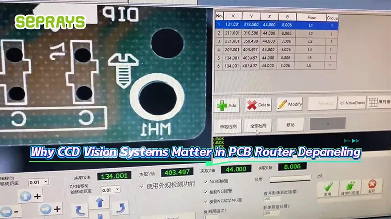
Why CCD Vision Systems Matter in PCB Router Depaneling
CCD Vision System technology has quietly become one of the most important upgrades in modern PCB router depaneling. Not because it makes machines look more advanced.But because PCB manufacturing tolerances are getting tighter every year. Smaller boards.Higher-density layouts.Components closer to cutting edges. Without accurate positioning, even a high-end depaneling machine can produce unstable results. And in 2026, instability is expensive. 🔍 What Does a CCD Vision System Actually Do? In simple terms, a CCD vision system helps the depaneling machine “see” the PCB. It automatically identifies: This allows the machine to correct positioning in real time. Especially important when: ⚙️ Why Manual Alignment Is No Longer Enough Years ago, manual positioning worked for many products. Today? Not always. Modern PCBAs often include: Even tiny alignment errors can cause: 💥 Common Problems Without CCD Alignment Factories often notice these issues first: 1. Inconsistent Cutting Accuracy The cutting path drifts slightly from the board edge. 2. Damage Near Sensitive Components Especially when parts are placed close to the depaneling line. 3. Longer Setup Time Operators spend more time adjusting fixtures manually. 4. High-Mix Production Delays Frequent model changes reduce efficiency. 💡 A Counterintuitive Insight Many people assume: “CCD systems are only needed
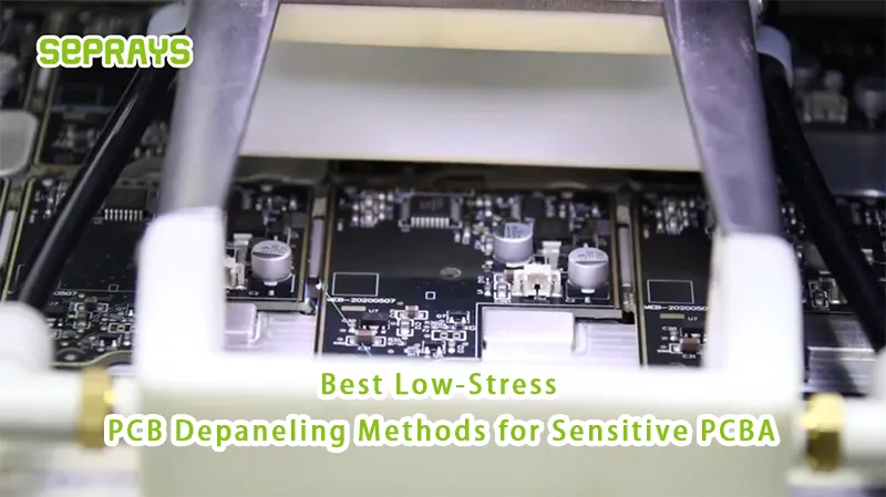
Best Low-Stress PCB Depaneling Methods for Sensitive PCBA
Best low-stress PCB depaneling methods for sensitive PCBA are becoming one of the most discussed topics in electronics manufacturing in 2026. Not because depaneling is new.But because PCB assemblies are getting more delicate every year. Smaller components.Thinner boards.Higher-density layouts. And less tolerance for stress. A process that worked five years ago may now create hidden reliability risks. 🔍 Why Sensitive PCBA Requires Low-Stress Depaneling Modern PCBAs often contain: These components are vulnerable to: The challenge is that damage is not always visible immediately. Sometimes failures appear only after: ⚙️ What Happens When Stress Is Too High? In real SMT production lines, common issues include: 1. Micro-Cracks in Solder Joints Especially around BGAs and ceramic capacitors. 2. PCB Warpage Thin boards deform during cutting. 3. Hidden Reliability Failures Products pass inspection but fail later in use. 4. Edge Damage and Delamination More common on multilayer or rigid-flex structures. 💥 Why Traditional Methods Struggle Many factories still rely on: These methods may work for simple boards. But sensitive PCBA reacts differently. Even small stress variations can affect yield. 💡 A Counterintuitive Insight Many engineers focus only on cutting force. But a lower force alone does not guarantee lower stress. For example: The

