.png)
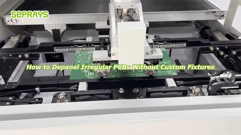
How to depanel high-density PCBs without damaging components? It’s a question that often comes up as designs get tighter and margins shrink. At first, everything looks fine on the SMT line. Then issues appear—cracked solder joints, lifted components, or unexplained failures during testing.
In many cases, the root cause is not assembly.
It’s the depaneling step.
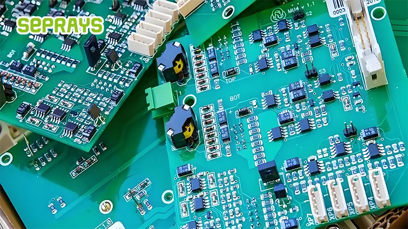
🔍 Why High-Density PCBs Are More Vulnerable
High-density PCBs are built for performance, not forgiveness.
They typically include:
- Components placed very close to board edges
- Fine-pitch ICs and BGAs
- Thin substrates or multi-layer structures
- Tight mechanical tolerances
This means even small mechanical stress can lead to:
- Micro-cracks
- Solder fatigue
- Component misalignment
The risk is higher.
And harder to detect early.
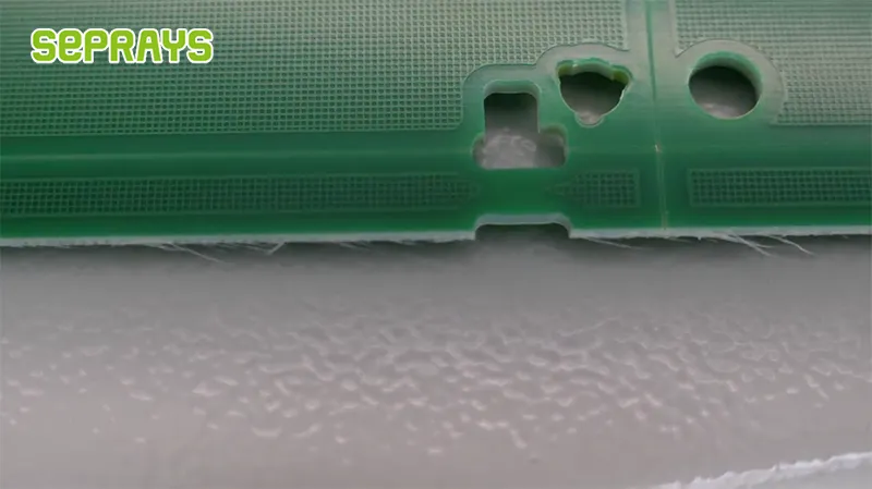
⚙️ Where Damage Usually Happens
Damage during depaneling is often subtle.
Common sources include:
- Mechanical force from cutting tools
- Vibration transferred to components
- Poor fixture support
- Incorrect cutting parameters
These factors combine.
And the result is often delayed failure, not immediate rejection.
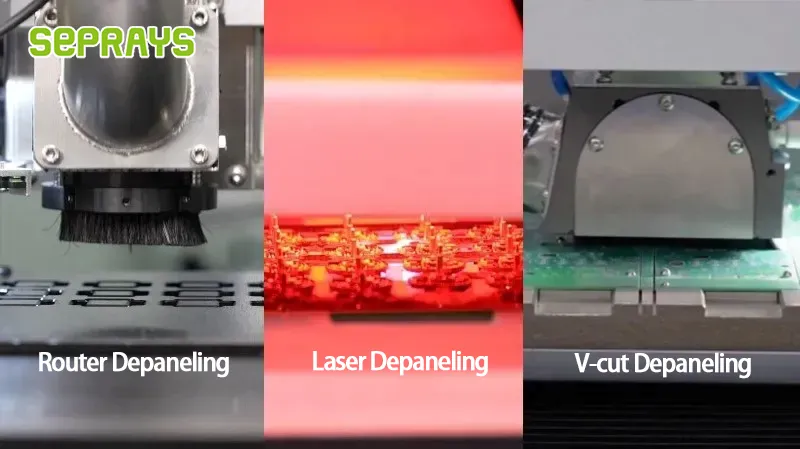
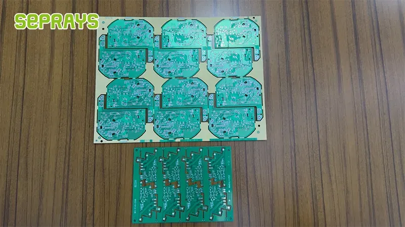
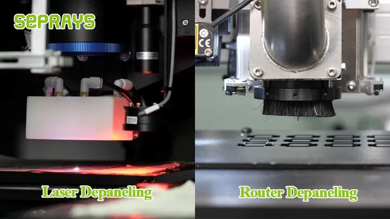
🧩 Choosing the Right Depaneling Method
Method selection is critical.
Here’s a practical comparison:
| Method | Stress Level | Precision | Suitability for High-Density PCBs |
|---|---|---|---|
| Saw Blade | Medium | Medium | Limited (risk near edges) |
| Router | Low-Medium | High | Good for complex layouts |
| Laser | Very Low | Very High | Ideal for sensitive components |
| V-Groove | Low | Medium | Only if spacing allows |
| Punching | Medium | Medium | Not recommended for dense boards |
For high-density designs, laser and optimized router depaneling are the most commonly used solutions.
💥 Common Pain Points from Production
Engineers working with dense PCBs often report:
- Edge components are cracking after depaneling
- Increased failure during ICT or functional testing
- Cosmetic edge damage affecting assembly
- Low yield despite stable SMT processes
These issues are frustrating because they are not always visible at first glance.
🛠️ Design-Level Prevention Strategies
The best solution starts at the design stage.
Consider:
- Keeping a safe distance between components and cutting lines
- Adding support rails or breakaway tabs
- Using proper V-groove depth, if applicable
- Avoiding sensitive component placement near edges
Design decisions reduce risk before manufacturing begins.
🔄 Process Optimization Techniques
On the production side, several improvements help:
- Adjust cutting speed and feed rate
- Use sharp, well-maintained tools
- Minimize vibration with stable fixtures
- Control dust and debris
Small parameter changes can significantly reduce damage.
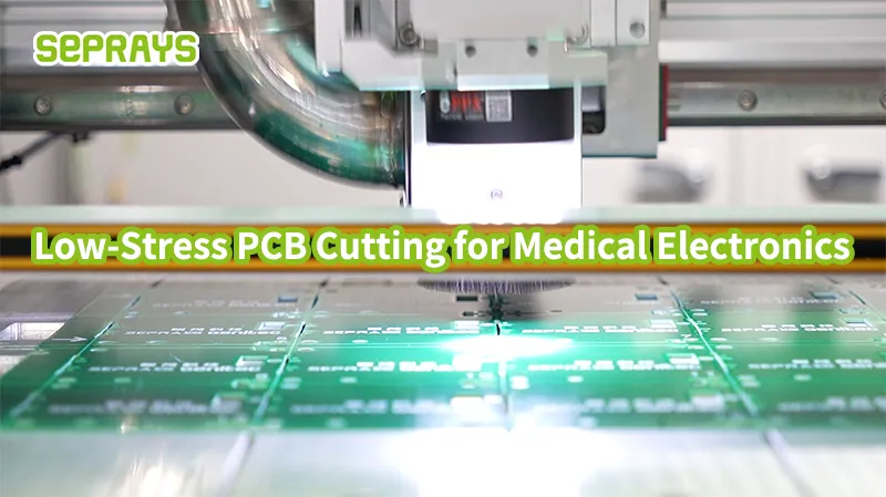
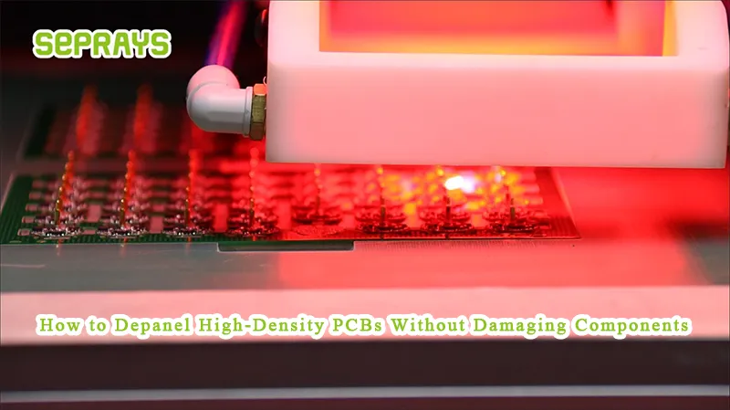
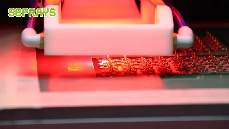
🚀 When to Use Laser Depaneling
Laser depaneling becomes necessary when:
- Components are extremely close to the edges
- PCB thickness is very thin
- Mechanical stress must be minimized
- High reliability is required
Because it is non-contact, it avoids the main cause of damage—mechanical force.
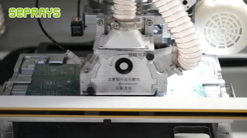
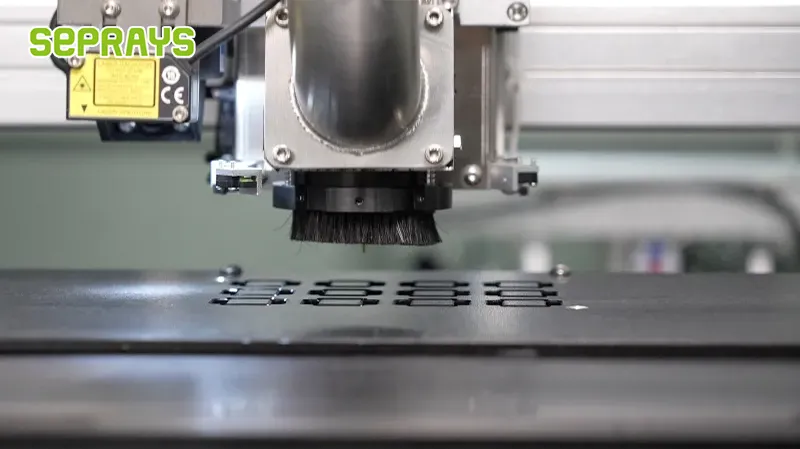
🔧 When Router Depaneling Is Enough
Router depaneling remains a practical option when:
- Board shapes are complex
- Moderate stress is acceptable
- Cost needs to be controlled
With proper optimization, it can deliver good results for many high-density applications.
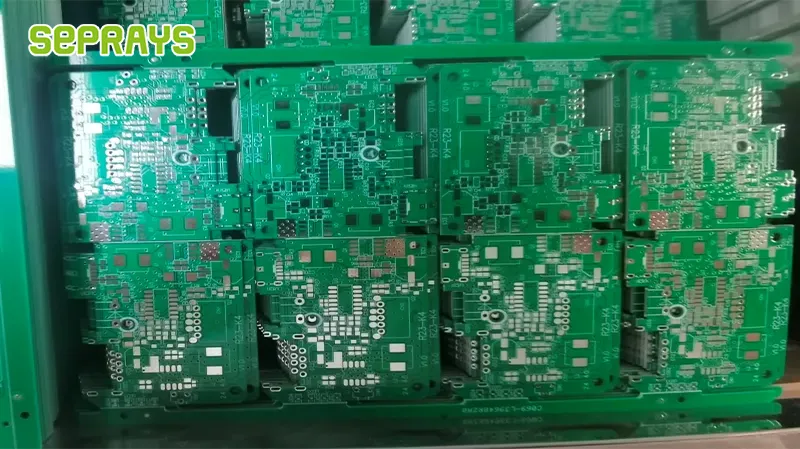
🧪 Case Study — Improving Yield for Dense PCBs
A manufacturer producing communication modules faced recurring failures.
Problems included:
- Cracked capacitors near PCB edges
- Inconsistent depaneling quality
- Rising rework costs
They worked with Seprays to improve the process.
Solution:
- Introduced laser depaneling for critical areas
- Optimized router parameters for the remaining sections
- Improved fixture design
Results:
- Significant reduction in component damage
- Higher yield
- More stable production
The key was combining the right methods.
💰 Cost vs Risk Consideration
High-density PCBs are high-value products.
Damage is expensive.
While laser systems cost more upfront, they help reduce:
- Scrap rates
- Rework
- Field failures
In many cases, the investment pays off through improved reliability.
🛠️ Practical Checklist for Engineers
Before finalizing your process:
- Are the components too close to the cutting edges?
- Is the chosen method low-stress enough?
- Are cutting parameters optimized?
- Is fixture support sufficient?
- Should a hybrid approach be considered?
These checks prevent costly mistakes.
🚀 Why Choose Seprays Group?
Seprays Group focuses on solving real depaneling challenges, especially for high-density and high-reliability PCB applications.
Seprays Group has been dedicated to PCB/FPC depaneling technology, providing a full range of solutions — including milling cutter depanelers, laser depanelers, V-groove depanelers, punching depanelers, and automated handling systems.
Their equipment is trusted by leading global manufacturers such as Foxconn, Flextronics, State Grid, Luxshare, Compal, Wistron, China Electronics, Quanta, CRRC, China Aerospace, OPPO, ZTE, and Bosch. These collaborations demonstrate proven performance in complex, large-scale production environments.
With strong application expertise, Seprays helps manufacturers reduce damage, improve yield, and achieve consistent quality.
If you are working with high-density PCBs and facing depaneling challenges, feel free to contact us.
WhatsApp: +8618929266433
E-mail: sales@seprays.com
❓ FAQ
1. Why are high-density PCBs more difficult to depanel?
Because components are closer to edges, making them more sensitive to stress.
2. Which method is safest for high-density boards?
Laser depaneling is the safest due to its non-contact process.
3. Can router depaneling still be used?
Yes, with proper optimization and when stress tolerance allows.
4. How to reduce component damage during depaneling?
Optimize parameters, improve fixtures, and choose low-stress methods.
5. Is laser depaneling worth the cost?
For high-value and sensitive PCBs, it often reduces overall production cost.