.png)
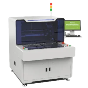


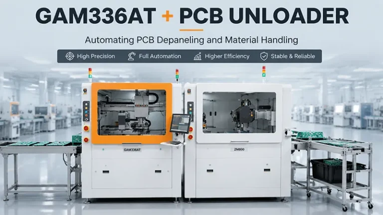
GAM336AT + PCB Unloader for Consumer Electronics Manufacturing: Automating PCB Depaneling and Material Handling
GAM336AT + PCB Unloader is designed for consumer electronics manufacturers that need more than just accurate PCB separation. In many modern factories, the real production challenge does not stop at cutting the PCB. It continues with: As consumer electronic products become smaller, smarter, and released faster, manufacturers are under increasing pressure to improve both quality and efficiency. A depaneling process that works well for small production volumes may become a bottleneck when demand increases. This is where automated PCB routing and material handling begin to create measurable value. 📱 Why Consumer Electronics Manufacturing Needs Smarter Depaneling Consumer electronics production has changed significantly in recent years. Products such as: are becoming smaller while containing more functions. This creates several manufacturing challenges.
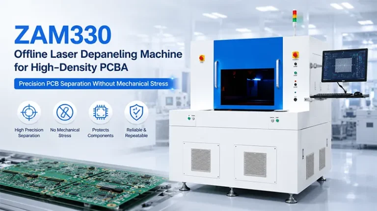
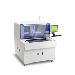
ZAM330 Offline Laser Depaneling Machine for High-Density PCBA: Precision PCB Separation Without Mechanical Stress
ZAM330 Offline Laser Depaneling Machine is becoming a practical choice for manufacturers producing high-density PCBAs where even slight mechanical stress can affect long-term product reliability. As electronic devices continue to shrink while integrating more functions, PCB layouts have become increasingly compact. Manufacturers place components closer to board edges, adopt more multilayer designs, and integrate expensive ICs or optical modules, leaving little room for processing errors. Many manufacturers have already invested in high-speed SMT lines and AOI systems. Yet, one production step still deserves more attention—PCB depaneling. The final separation process may only take seconds, but it can determine whether a finished product performs reliably for years. This article shares practical observations from modern electronics manufacturing, explains where laser depaneling fits,
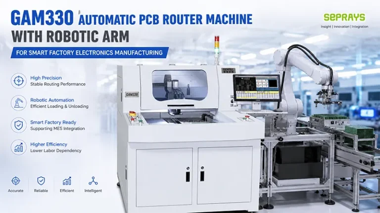
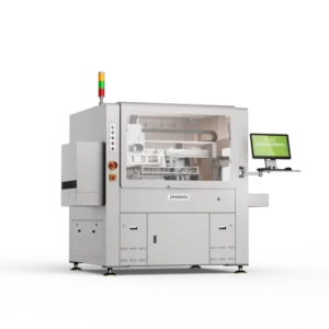
GAM330 Automatic PCB Router Machine with Robotic Arm for Smart Factory Electronics Manufacturing
In modern electronics factories, the biggest challenge is not always increasing production speed. Many manufacturers are finding that GAM330 Automatic PCB Router Machine solutions become important when they need stable quality, lower manual handling, and better production consistency. A PCB router process may look simple from the outside: place the board, cut the outline, remove the finished parts. However, in real production environments, problems often appear after scaling up. Operators need to repeat the same movements hundreds or thousands of times every day. Small positioning errors, dust contamination, tool wear, and inconsistent handling can gradually affect yield. This is why more factories are exploring automated PCB routing systems with robotic integration, especially for smart factory production lines. The question is

Seprays Shares a Summer Appreciation Gift with Every Employee
As the summer heat reaches its peak, Seprays prepared a simple yet meaningful surprise to thank every member of our team for their continued dedication and hard work. This year, more than 750 kg of fresh watermelons were distributed across the company, ensuring that every employee—from every department and every team—received a refreshing summer gift. A Simple Gesture of Appreciation At Seprays, we believe that every achievement begins with the people behind it. Whether working in research and development, manufacturing, quality control, sales, customer service, or administration, every colleague plays an important role in delivering reliable PCB depaneling solutions to customers worldwide. While a watermelon may seem like a small gift, it reflects something much more meaningful—our appreciation for the

