.png)
 English
  Spanish
  Japanese
  Korean
  Russian
  Chinese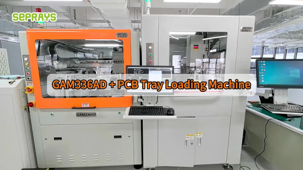
Dual-Spindle PCB Depaneling for Higher Production Efficiency and Automated Tray Loading
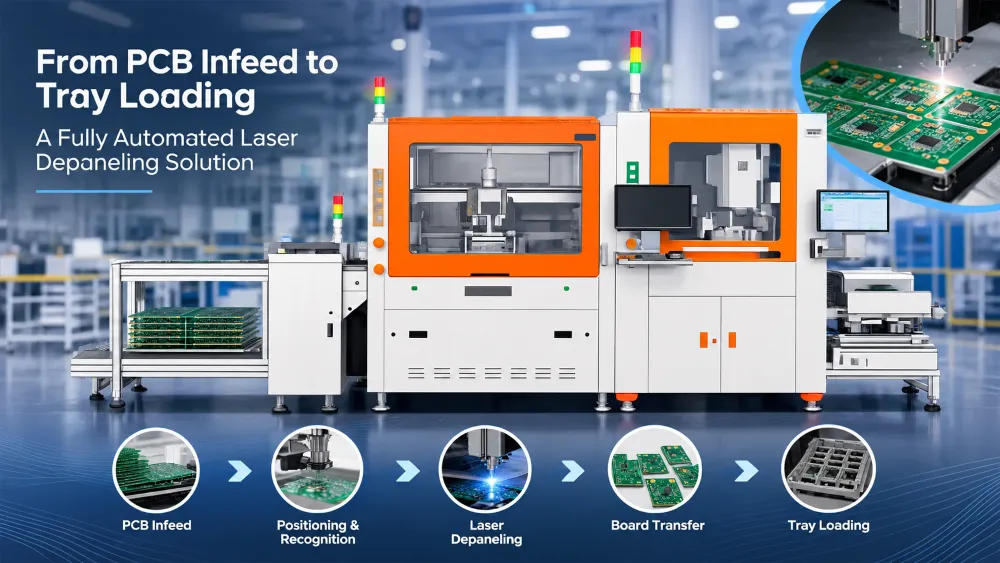
Dual-spindle PCB depaneling is worth considering when a production line needs more output but cannot afford extra manual handling or a larger workstation footprint. In electronics manufacturing, cutting is only part of the cycle. Boards still need to be positioned, separated, collected, and transferred to the next process. When these steps fall behind, a fast machine alone will not solve the bottleneck. 🔍 Why Does Production Slow Down? Imagine an overseas semiconductor-related electronics manufacturer producing assembled circuit boards for industrial or consumer electronics. Orders are increasing, but operators spend too much time moving panels, unloading finished boards, and preparing the next cycle. The cutting machine may be capable of working faster, yet the overall line remains constrained by handling time. Common issues include: The practical question is not simply how fast the spindle runs. It is how many acceptable boards the complete process can deliver per hour. ⚙️ How Does a Dual-Spindle System Help? A dual-spindle configuration allows two cutting spindles to work within a coordinated process. Depending on the machine design and programmed sequence, this can increase cutting capacity and reduce idle time. For suitable PCB designs, the GAM336AD dual-spindle solution from Seprays combines milling-based separation with inline automation
Which PCB Depaneling Machine Manufacturers Serve International Electronics Manufacturers?
PCB depaneling machine manufacturers serve different needs across the electronics industry. Some focus on routing and milling, while others specialize in laser processing, V-groove separation, or integrated production-line automation. For international electronics manufacturers, choosing a supplier involves more than comparing machine prices. Cutting quality, production compatibility, technical support, and long-term operating costs all deserve attention. 🔍 Which Manufacturers Should You Evaluate? There is no single manufacturer that fits every PCB application. The following companies are starting points for a supplier shortlist, rather than a definitive industry ranking. Before requesting quotations, confirm that each supplier supports your specific board design, production volume, installation region, and service requirements. ⚙️ How Do Their Solutions Differ? The machine technology often matters more than the supplier’s general reputation. Technology Typical application What to verify Router / milling Complex outlines and curved cutting paths Edge quality, cutter life, dust extraction Laser Fine features and reduced mechanical cutting force Material compatibility, heat effects, fume control V-groove Panels with pre-scored separation lines Groove geometry, component clearance Punching Repetitive designs compatible with dedicated tooling Tooling cost and product-change flexibility Inline automation High-volume, connected production Transfer accuracy, cycle time, line integration A useful correction to a common assumption: laser is
What Does Seprays Specialize In?
Seprays specializes in PCB/FPC depaneling technology and automated manufacturing solutions. For electronics manufacturers, the real challenge is not simply separating a PCB from a panel. It is finding a method that protects components, maintains cutting consistency, and fits the existing production workflow. If you are comparing equipment suppliers, understanding the available technologies is a practical place to start. 🔍 What Does Seprays Actually Do? Seprays develops and manufactures equipment for separating printed circuit boards (PCBs) and flexible printed circuit boards (FPCs). Its solutions cover several production needs: The key point is that these methods aren’t interchangeable. The right choice depends on board material, thickness, component clearance, panel design, required output, and acceptable edge quality. ⚙️ How Do You Choose the Right Technology? A common purchasing mistake is to compare machine prices before confirming the cutting method. A lower initial price may not represent the lower total cost if the process creates excessive rework, requires frequent manual handling, or cannot accommodate future product changes. Technology Often suitable for Key consideration Milling cutter Complex outlines and curved paths Cutter wear, dust extraction, and tool paths Laser Fine features and low mechanical cutting force Material compatibility, heat effects, and fume extraction V-groove Pre-scored
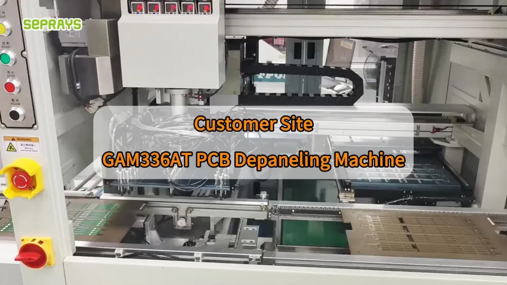
Inline PCB Depaneling in Action: A Real-World Customer Application
Inline PCB depaneling becomes interesting when production is no longer limited by the cutting process itself, but by everything happening around it. In a high-volume electronics factory, operators may still need to load panels, align boards, separate finished PCBs, collect waste, and move products to the next process. Each action looks small. Across thousands of cycles, it becomes a production problem. This is where an overseas semiconductor-related electronics manufacturer started reviewing its depaneling process. 🔍 The Production Problem Was Not Just Cutting The customer was producing assembled PCBs for applications where consistency mattered more than simply achieving a fast cutting cycle. The existing workflow involved several manual steps. Operators had to handle panels between processes, position them correctly, and move separated boards to the next stage. The main concerns were familiar: The question was not simply: “Can the PCB be separated?” It was: “Can the separation process become part of the production line?” ⚙️ Why an Inline Routing Approach Made Sense The PCB designs included different outlines and sections that were not always suitable for a simple straight-line separation method. Milling offered more flexibility. A programmed cutter can follow straight lines, L-shaped paths, U-shaped paths, circles, arcs, and other board

🇨🇳 Celebrating China’s National Day 2026
October 1 marks China’s National Day, a time to reflect on the country’s journey, achievements, and continued development. In 2026, China celebrates the 77th anniversary of the founding of the People’s Republic of China. Over the decades, the country has experienced significant changes across manufacturing, technology, infrastructure, and international trade. For Seprays, this occasion is also an opportunity to appreciate the people, partners, and customers who have been part of our journey. As a manufacturer serving customers in international markets, we continue to focus on practical innovation, manufacturing capabilities, and long-term cooperation across borders. From PCB depaneling solutions to automated production equipment, our work is closely connected with the development of modern electronics manufacturing. 🌏 Looking Toward the Future A national celebration is not only about looking back. It is also a moment to look ahead. As electronics manufacturing continues to evolve, new requirements are emerging around automation, precision, production efficiency, and process consistency. We will continue to explore how manufacturing technology can respond to these changing needs. On this special occasion, Seprays would like to wish our employees, customers, business partners, and friends around the world a Happy China National Day. 1949–2026 | 77 Years One Nation · One
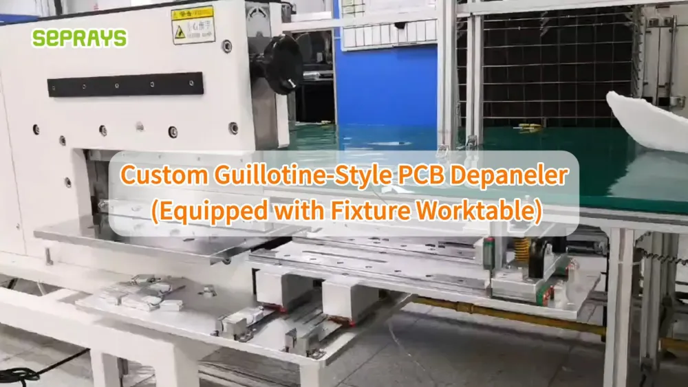
Custom PCB Depaneler for Safer Production: A Real-World Customer Application
Custom PCB Depaneler is not always about building a completely new machine. In many production lines, the real requirement is much simpler: make the existing PCB separation process safer, more repeatable, and easier for operators to control. This becomes especially important when a PCB has a V-groove, sensitive components close to the cutting line, or a production team that needs to run the same operation repeatedly throughout the day. A recent customer application involving an overseas semiconductor manufacturer is a good example. The customer was not simply looking for a machine that could cut a PCB. They wanted to reduce the risk of operator error while keeping the separation process stable. That changed the way the solution was designed. 🔎 The Problem Was Not Simply “How to Cut the PCB” At first glance, PCB depaneling looks straightforward. Place the panel. Align it. Cut along the V-groove. Remove the separated board. But production tells a different story. When operators repeat the same movement hundreds or thousands of times, small differences become important. A board may not be positioned correctly. An operator may put their hand too close to the cutting area. Different PCB thicknesses may require different settings. A worn blade