.png)
 Korean
  English
  Spanish
  Japanese
  Russian
  Chinese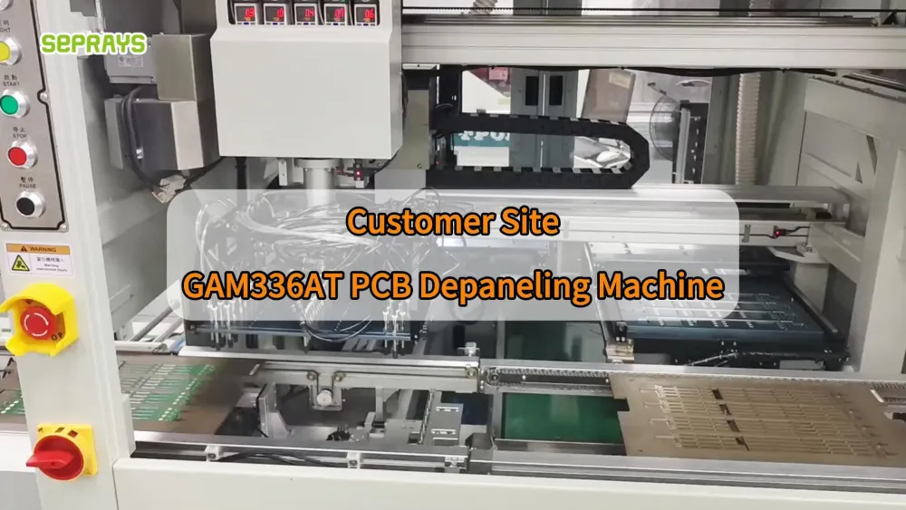
Inline PCB Depaneling in Action: A Real-World Customer Application
Inline PCB depaneling becomes interesting when production is no longer limited by the cutting process itself, but by everything happening around it. In a high-volume electronics factory, operators may still need to load panels, align boards, separate finished PCBs, collect waste, and move products to the next process. Each action looks small. Across thousands of cycles, it becomes a production problem. This is where an overseas semiconductor-related electronics manufacturer started reviewing its depaneling process. 🔍 The Production Problem Was Not Just Cutting The customer was producing assembled PCBs for applications where consistency mattered more than simply achieving a fast cutting cycle. The existing workflow involved several manual steps. Operators had to handle panels between processes, position them correctly, and move separated boards to the next stage. The main concerns were familiar: The question was not simply: “Can the PCB be separated?” It was: “Can the separation process become part of the production line?” ⚙️ Why an Inline Routing Approach Made Sense The PCB designs included different outlines and sections that were not always suitable for a simple straight-line separation method. Milling offered more flexibility. A programmed cutter can follow straight lines, L-shaped paths, U-shaped paths, circles, arcs, and other board

🇨🇳 Celebrating China’s National Day 2026
October 1 marks China’s National Day, a time to reflect on the country’s journey, achievements, and continued development. In 2026, China celebrates the 77th anniversary of the founding of the People’s Republic of China. Over the decades, the country has experienced significant changes across manufacturing, technology, infrastructure, and international trade. For Seprays, this occasion is also an opportunity to appreciate the people, partners, and customers who have been part of our journey. As a manufacturer serving customers in international markets, we continue to focus on practical innovation, manufacturing capabilities, and long-term cooperation across borders. From PCB depaneling solutions to automated production equipment, our work is closely connected with the development of modern electronics manufacturing. 🌏 Looking Toward the Future A national celebration is not only about looking back. It is also a moment to look ahead. As electronics manufacturing continues to evolve, new requirements are emerging around automation, precision, production efficiency, and process consistency. We will continue to explore how manufacturing technology can respond to these changing needs. On this special occasion, Seprays would like to wish our employees, customers, business partners, and friends around the world a Happy China National Day. 1949–2026 | 77 Years One Nation · One
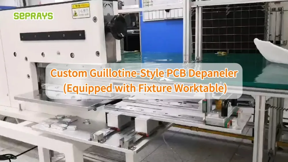
Custom PCB Depaneler for Safer Production: A Real-World Customer Application
Custom PCB Depaneler is not always about building a completely new machine. In many production lines, the real requirement is much simpler: make the existing PCB separation process safer, more repeatable, and easier for operators to control. This becomes especially important when a PCB has a V-groove, sensitive components close to the cutting line, or a production team that needs to run the same operation repeatedly throughout the day. A recent customer application involving an overseas semiconductor manufacturer is a good example. The customer was not simply looking for a machine that could cut a PCB. They wanted to reduce the risk of operator error while keeping the separation process stable. That changed the way the solution was designed. 🔎 The Problem Was Not Simply “How to Cut the PCB” At first glance, PCB depaneling looks straightforward. Place the panel. Align it. Cut along the V-groove. Remove the separated board. But production tells a different story. When operators repeat the same movement hundreds or thousands of times, small differences become important. A board may not be positioned correctly. An operator may put their hand too close to the cutting area. Different PCB thicknesses may require different settings. A worn blade
Celebrating Mid-Autumn Festival Together at Seprays & Genitec
Before the Mid-Autumn Festival, there is one tradition we never want to miss at Seprays & Genitec: making mooncakes together. We have kept this tradition for many years. It is a simple activity, but it has become one of the moments our team looks forward to every year. This year, the mooncake ingredients were prepared by Guangzhou Restaurant, with a variety of flavors including custard, chestnut, mixed nuts, lotus seed paste with salted egg yolk, and even Dove chocolate. And then there was one particularly unusual flavor: preserved egg mooncakes. Before we even started, the discussion had already begun. “Which flavor will be the best?” “Who is brave enough to try the preserved egg one first?” The room quickly filled with laughter. 🥮 Everyone Becomes a Mooncake Maker Once we started making the mooncakes, everyone became surprisingly focused. Some colleagues were already experienced at wrapping the fillings, producing beautifully shaped mooncakes one after another. For those making mooncakes for the first time, things were a little different. Some came out slightly uneven after being removed from the mold. Others had a little filling showing through. But somehow, when you make something yourself, it always looks pretty good. After a busy
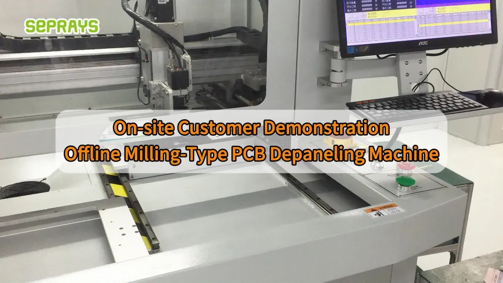
PCB Depaneling for Leading Smartphone Manufacturers: A Real-World Customer Application
PCB depaneling becomes much less forgiving when the board is part of a modern smartphone. The boards are smaller. Components are packed closer together. Production volumes are high. And a small problem at the separation stage can create much more work downstream. That is why a smartphone PCB should not be treated simply as “another PCB to cut.” For a semiconductor and consumer-electronics manufacturing application serving the smartphone supply chain, the production team was looking for a more repeatable way to separate small multi-connected boards while keeping the process stable during continuous production. The challenge was not simply cutting faster. It was finding a process that could keep up with production without making board handling and quality inspection more complicated. 🔍 What Makes Smartphone PCB Depaneling Different? A smartphone PCB can leave little room for process variation. Components may be positioned close to the board edge. The board outline can include curves, corners, slots, or multiple connected sections. At the same time, production quantities can be substantial. This creates several practical concerns: These questions are more useful than simply asking for the machine’s maximum cutting speed. 🏭 The Customer Production Challenge In the customer application, the production team was dealing
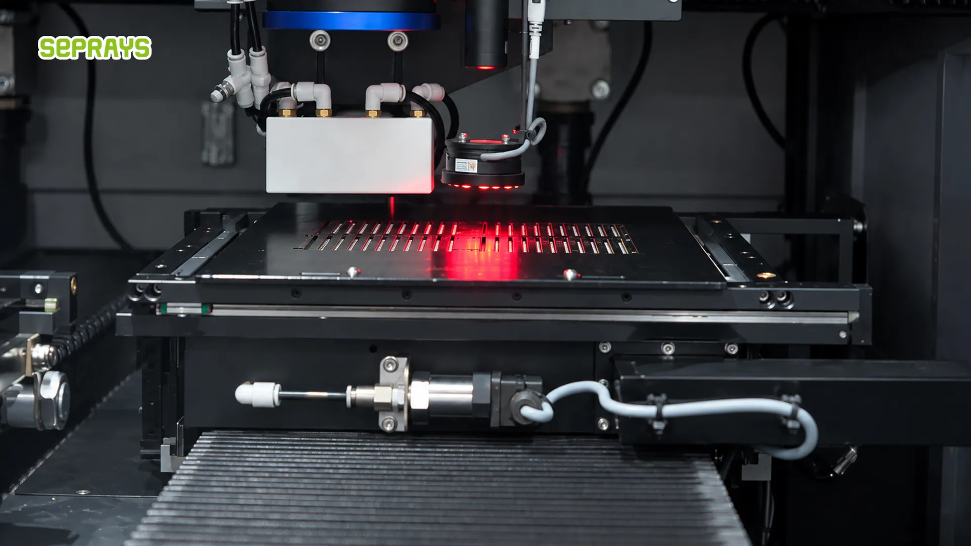
From PCB Infeed to Tray Loading: A Fully Automated Laser Depaneling Solution
Laser depaneling becomes much more interesting when it is no longer a standalone cutting operation. In a modern electronics factory, the question is often bigger than how quickly a PCB can be separated. What happens before cutting? How is the PCB positioned? How are separated boards transferred? Who loads the trays? And what happens when the tray becomes full? For a semiconductor-related electronics manufacturer, these questions became increasingly important as production volume increased and manual handling started to interrupt an otherwise stable process. The solution was not simply a faster laser. It was a connected workflow—from PCB infeed to automated tray loading. 🏭 The Customer Production Challenge The customer manufactures electronic assemblies for semiconductor-related equipment. The existing process involved several separate steps: PCB infeed → positioning → laser separation → manual collection → manual tray loading Each step worked independently. The problem appeared between the steps. Operators had to move boards manually. Finished boards accumulated while waiting for tray loading. Empty trays needed to be prepared. Full trays had to be removed. With higher production volume, these small interruptions became more noticeable. There was another concern. The PCB assemblies contained sensitive components, so reducing unnecessary mechanical contact during separation and