.png)


How to Depanel High-Density PCBs Without Damaging Components
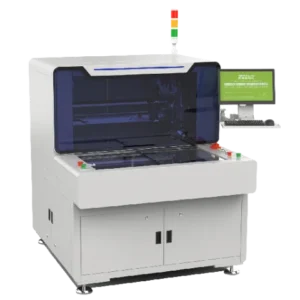
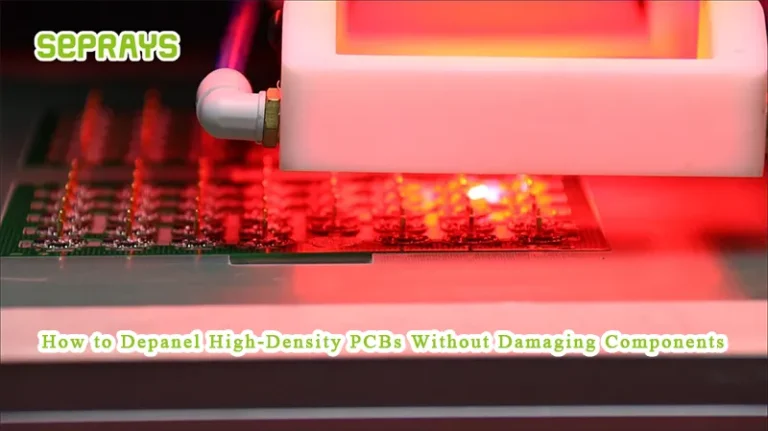
How to depanel high-density PCBs without damaging components? It’s a question that often comes up as designs get tighter and margins shrink. At first, everything looks fine on the SMT line. Then issues appear—cracked solder joints, lifted components, or unexplained failures during testing. In many cases, the root cause is not assembly.It’s the depaneling step. 🔍 Why High-Density PCBs Are More Vulnerable High-density PCBs are built for performance, not forgiveness. They typically include: This means even small mechanical stress can lead to: The risk is higher.And harder to detect early. ⚙️ Where Damage Usually Happens Damage during depaneling is often subtle. Common sources include: These factors combine. And the result is often delayed failure, not immediate rejection. 🧩 Choosing the
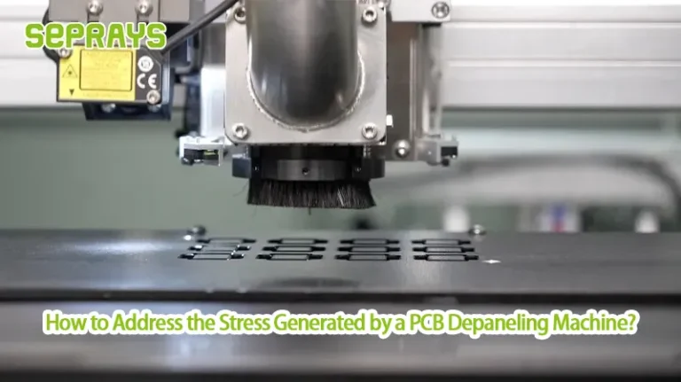
How to Address the Stress Generated by a PCB Depaneling Machine?
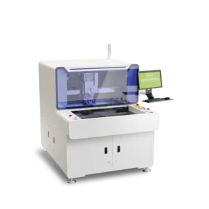
How to address the stress generated by a PCB depaneling machine? It’s a question many engineers don’t ask—until defects start showing up. Cracked edges. Intermittent failures. Reduced yield with no obvious root cause. In many cases, the issue isn’t assembly.It starts with depaneling. 🔍 Where Does Depaneling Stress Come From? Stress is introduced during the separation process. Different sources include: Even small forces can affect: The challenge is not eliminating stress—but controlling it. ⚙️ How Different Depaneling Methods Affect Stress Not all machines behave the same. Here’s a simplified comparison: Method Stress Level Key Characteristics Saw Blade Medium High speed, mechanical contact Router Low-Medium Controlled cutting, flexible paths Laser Very Low Non-contact, minimal mechanical impact V-Groove Low Controlled breaking along
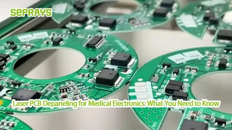
Laser PCB Depaneling for Medical Electronics: What You Need to Know
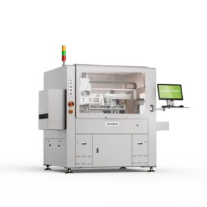
Laser PCB depaneling for medical electronics is not something most teams think about at the start of a project. It usually becomes important later, when edge defects appear, or when reliability testing starts to fail without a clear reason. In medical devices, small issues don’t stay small.They show up in performance.And sometimes, in compliance. 🏥 Why Medical Electronics Require Extra Care Medical PCBs are different from standard consumer products. They often involve: These boards are used in devices where failure is not acceptable. So the depaneling process must avoid introducing any hidden damage. ⚙️ What Makes Laser Depaneling Stand Out Laser PCB depaneling is a non-contact process. No mechanical force.No blade pressure. That changes everything. Key advantages include: For medical
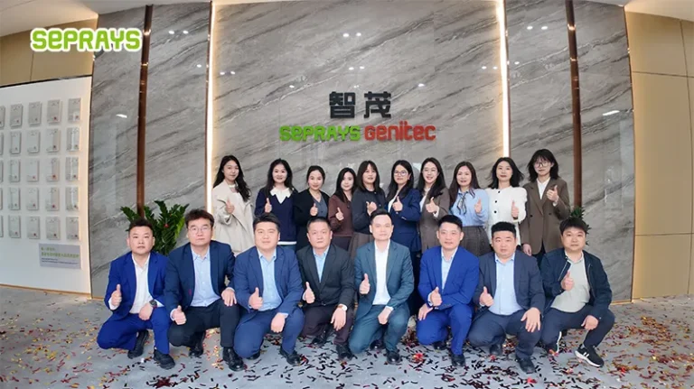
Not a New Starting Point, but a New Height: Seprays Suzhou Branch Upgrades and Relocates
Many of our clients are unaware that… Seprays’ Suzhou branch established its presence there as early as 2022. However, this time, things are different. On March 30, 2026, we officially relocated and upgraded our facility.This isn’t merely a simple change of office space; rather, it represents—Bringing our “service capabilities” directly to our clients’ doorsteps. Why the upgrade? Over the past few years, we have been serving an ever-growing number of clients across East China: And their requirements have become increasingly consistent: Previously, many matters required back-and-forth communication.Now, we have fully established our “on-site capabilities” to handle them directly. What makes the Suzhou branch different? What does this mean for you? If you are currently facing any of these issues: Then

