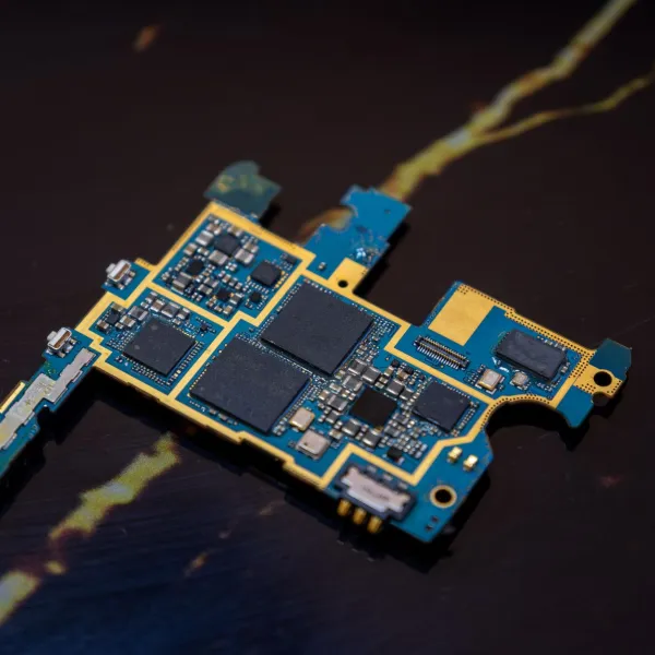
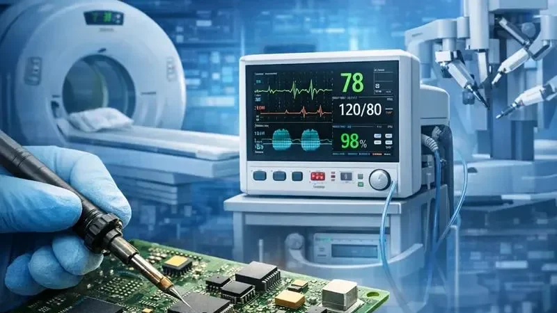
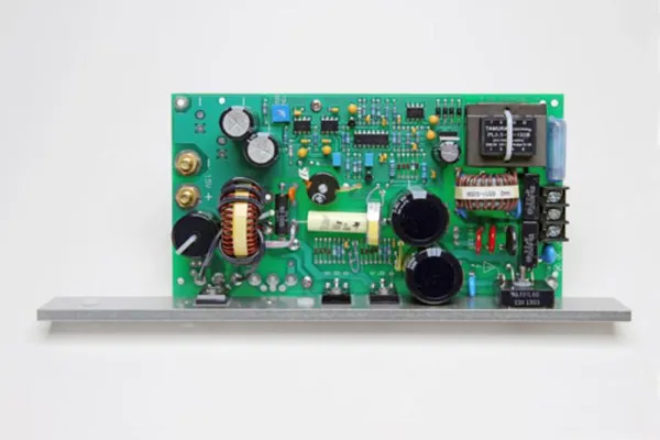
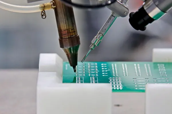
Implant devices, monitoring systems, and surgical electronics
Real Challenges:
Zero tolerance for mechanical stress
Strict cleanliness (no dust contamination)
Extremely high reliability requirements
Engineering Risks:
Hidden PCB damage (latent defects)
Contamination affecting performance
Compliance failure
Recommended Solution:
Laser depaneling (UV laser preferred)
Secondary dust cleaning system
AOI / visual inspection
Why This Works:
Achieves stress-free cutting + ultra-clean process
Typical Products:
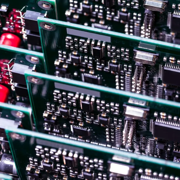
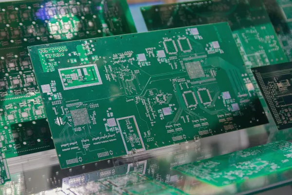
ECU, sensors, power control modules
Real Challenges:
Thick PCB / multi-layer boards
Complex outlines
Long-term reliability requirements
Engineering Risks:
Delamination
Inconsistent edge quality
Tool wear is affecting consistency
Recommended Solution:
Router or saw blade depaneling
Heavy-duty machine structure
Automated handling + inspection
Why This Works:
Ensures stable cutting + long-term consistency
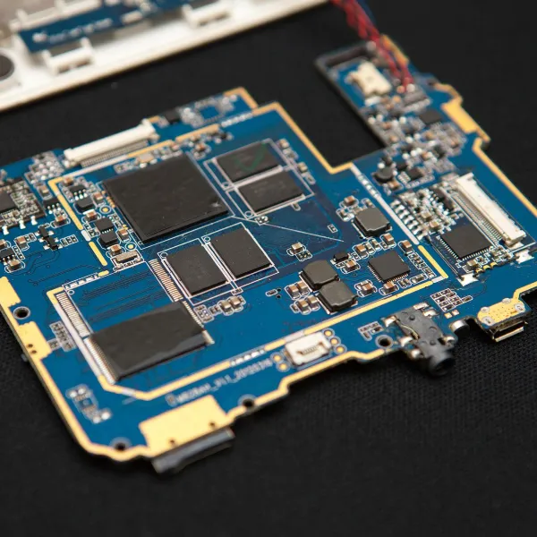
Typical Products:
Power supplies, control systems, automation equipment
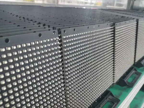
Real Challenges:
Large PCB size
Thick material
Lower volume but high reliability
Engineering Risks:
Warping during cutting
Uneven edges
Low efficiency in manual processes
Recommended Solution:
Router depaneling (high stability)
Manual + semi-auto solutions
Dust control system
Why This Works:
Provides flexibility + stable cutting for large boards
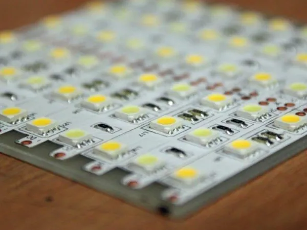
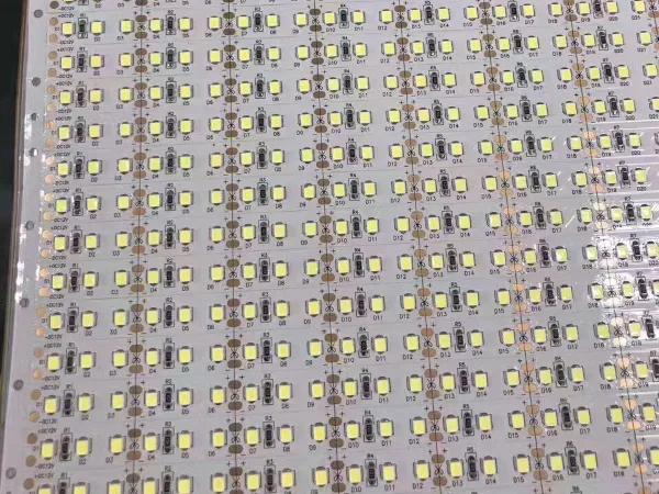
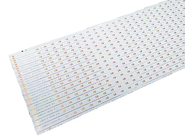
Typical Products:
LED strips, lighting panels, aluminum PCBs
Real Challenges:
Aluminum substrate (hard material)
Long boards/strip boards
High-speed production
Engineering Risks:
Tool wear
Rough edges
Heat impact
Recommended Solution:
Saw blade depaneling
V-Cut for linear boards
High-speed automation
Why This Works:
Optimized for speed + durability in hard materials
Typical Products:
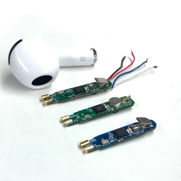
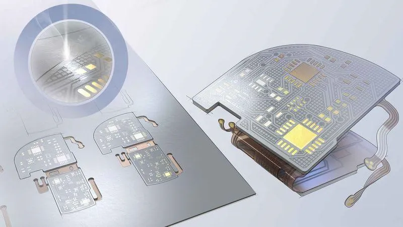
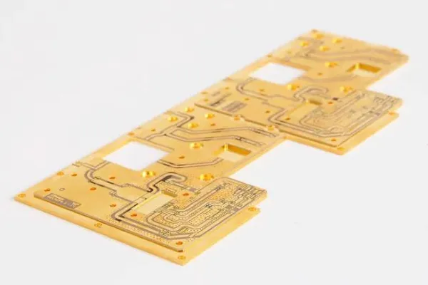
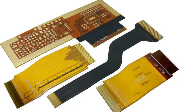
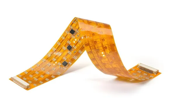
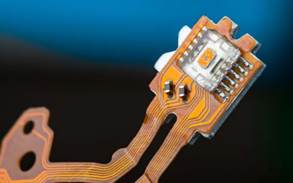
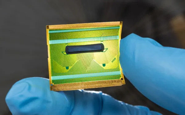
Flexible circuits, foldable devices, camera modules
Real Challenges:
Ultra-thin materials
Easily deformed
Extremely sensitive to stress
Engineering Risks:
Deformation
Edge burning or tearing
Precision loss
Recommended Solution:
Laser depaneling (non-contact)
High-precision motion control
Vision alignment system
Why This Works:
Delivers maximum precision with zero deformation
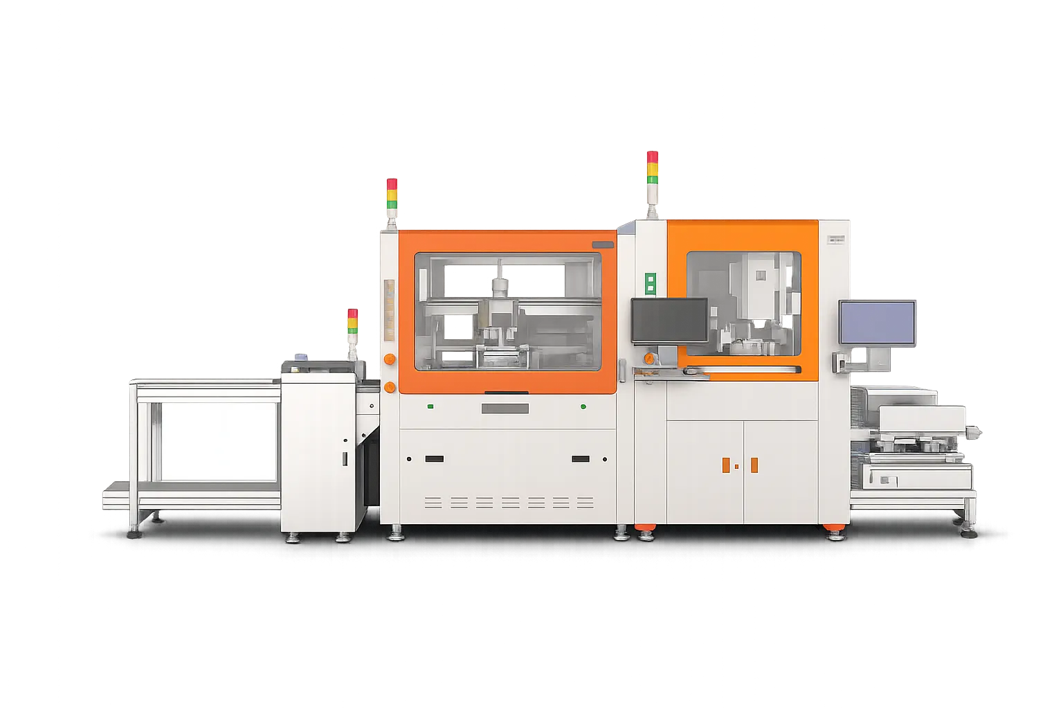
Applicable to ALL industries above
Full Process Includes:
PCB loading system
Depaneling (Laser / Router / V-Cut / Punching)
Unloading & tray arrangement
Secondary dust cleaning
AOI inspection
Core Value:
Reduce labor, improve yield, and stabilize production quality.
Still not sure which solution fits your PCB?
Different industries require different depaneling strategies.
Send us your PCB file or application —
we’ll recommend the most suitable process based on your product.
.png)

