.png)
 English
  Spanish
  Japanese
  Korean
  Russian
  Chinese
PCB depaneling becomes much less forgiving when the board is part of a modern smartphone.
The boards are smaller.
Components are packed closer together.
Production volumes are high.
And a small problem at the separation stage can create much more work downstream.
That is why a smartphone PCB should not be treated simply as “another PCB to cut.”
For a semiconductor and consumer-electronics manufacturing application serving the smartphone supply chain, the production team was looking for a more repeatable way to separate small multi-connected boards while keeping the process stable during continuous production.
The challenge was not simply cutting faster.
It was finding a process that could keep up with production without making board handling and quality inspection more complicated.
🔍 What Makes Smartphone PCB Depaneling Different?
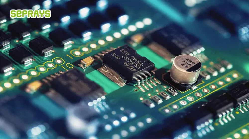
A smartphone PCB can leave little room for process variation.
Components may be positioned close to the board edge.
The board outline can include curves, corners, slots, or multiple connected sections.
At the same time, production quantities can be substantial.
This creates several practical concerns:
- How accurately can the cutting path follow the PCB outline?
- How stable is the PCB during separation?
- How often does the cutter need to be changed?
- Can operators load and unload without creating a bottleneck?
- How is cutting dust controlled?
- Does edge quality remain consistent after continuous production?
These questions are more useful than simply asking for the machine’s maximum cutting speed.
🏭 The Customer Production Challenge
In the customer application, the production team was dealing with small multi-connected PCB assemblies used in smartphone-related electronics.
The previous process involved more manual intervention than the team wanted.
An operator had to handle the panels.
Positioning needed to be checked.
After separation, boards had to be collected and transferred to the next process.
None of these tasks seemed particularly difficult.
But at production scale, repetition changes the equation.
If an operator handles hundreds or thousands of boards, even a few seconds per cycle becomes measurable labor time.
More importantly, manual handling introduces another variable into the process.
The customer wanted to reduce that variation while maintaining the flexibility needed for different PCB designs.
⚙️ Why Routing Was Considered
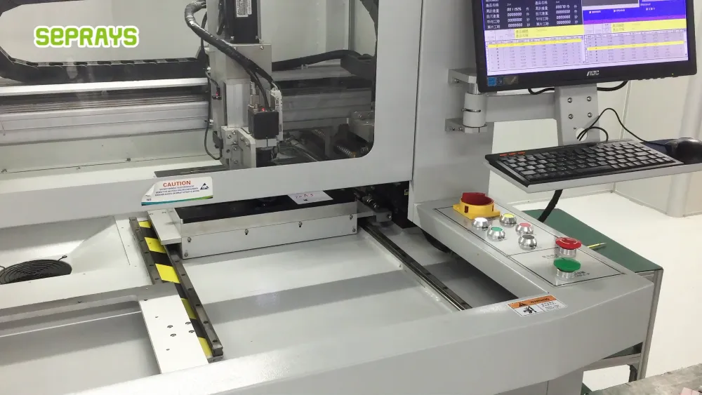
The team compared several common depaneling methods.
| Requirement | Routing | V-Groove | Laser | Punching |
|---|---|---|---|---|
| Complex PCB contours | Strong | Limited | Strong | Limited |
| Straight-line separation | Good | Excellent | Good | Good |
| Programmable path | Yes | Limited | Yes | Limited |
| Mechanical contact | Yes | Yes | No | Yes |
| High-mix production | Suitable | Suitable for compatible designs | Suitable | More tooling-dependent |
| Tooling flexibility | High | High | High | Lower |
| Process residue | Dust extraction needed | Generally low | Fume/extraction control | Generally low |
For this application, routing offered a practical balance.
The cutting path could be programmed according to the PCB outline.
It also avoided the need to design a dedicated punching die for every new contour.
But there was an important condition.
The process still needed to be validated against the actual PCB material, thickness, component placement, and required edge quality.
🎯 Positioning Comes Before Cutting
One lesson from production applications is easy to overlook:
Cutting accuracy starts with positioning accuracy.
If the panel is not correctly located, even a precise cutting system cannot produce the intended result.
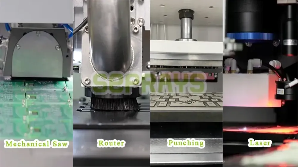
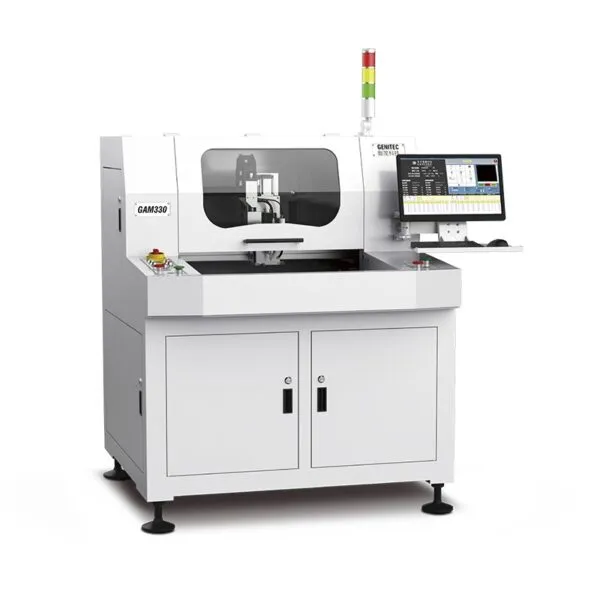
The GAM330 uses a high-speed CCD vision automatic calibration system to identify the PCB position before cutting. The system can also support cutting-path simulation and offline programming.
For the production team, this means the machine does not have to rely solely on manually aligned panels.
The process can instead follow a defined positioning and calibration routine.
That becomes especially useful when multiple PCB designs share the same production environment.
🛠️ Cutting Small and Complex PCB Outlines
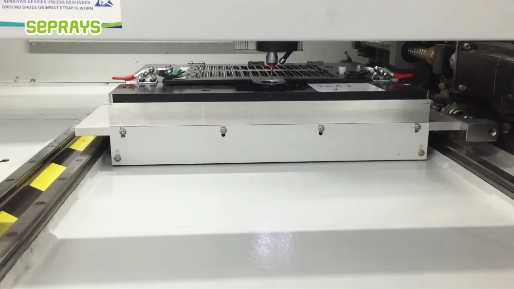
Once positioned, the programmed routing path follows the required PCB contour.
The GAM330 supports straight lines as well as L-shaped, U-shaped, circular, and arc cutting paths. Its published specifications list a cutting area of 300 × 350 mm and adjustable cutting speeds up to 100 mm/s.
These specifications are useful.
But they are not the whole story.
For a smartphone PCB, engineers also need to consider:
Component clearance → board support → cutter diameter → cutting depth → feed rate → spindle speed → dust extraction
Changing one parameter can affect another.
For example, increasing cutting speed may improve throughput, but it does not automatically improve the process.
If vibration increases or the cutter wears faster, the apparent productivity gain may disappear.
🔄 Dual Worktables and Production Flow
Another practical consideration is what happens while one PCB is being processed.
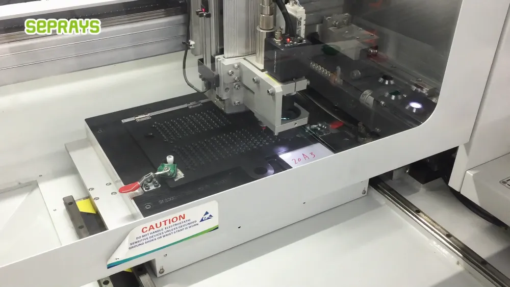
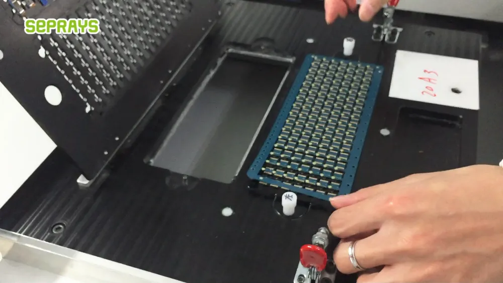
The GAM330 uses a dual-worktable configuration. According to the product specifications, the tables can support simultaneous loading and cutting operations, or be combined into a single larger worktable for larger PCBs.
This creates an opportunity to reduce waiting between operations.
Instead of treating loading and cutting as completely separate activities, the production workflow can overlap them where the application allows.
This is a small design choice with a potentially important production effect.
The machine does not necessarily need to cut faster.
It may simply need to spend less time waiting.
🔧 Cutter Management Matters at Production Scale
A cutter is a consumable tool.
That sounds obvious.
But in high-volume smartphone-related production, tool management can become part of quality control.
A worn cutter can influence edge appearance, cutting behavior, and process stability.
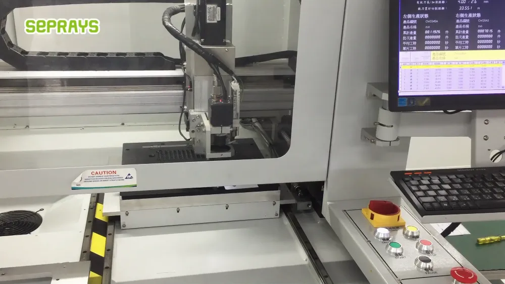
The GAM330 includes automatic tool changing and milling-tool detection. The system can also detect conditions such as cutter slippage, breakage, and improper installation, according to the current product information.
This does not remove the need for maintenance.
It changes how maintenance can be managed.
Instead of waiting for an obvious cutting problem, production teams can incorporate tool condition and usage into routine process management.
🧹 Managing Dust Without Creating a New Problem
Mechanical routing creates cutting debris.
For smartphone electronics, cleanliness matters because the separated boards still need to move into subsequent manufacturing processes.
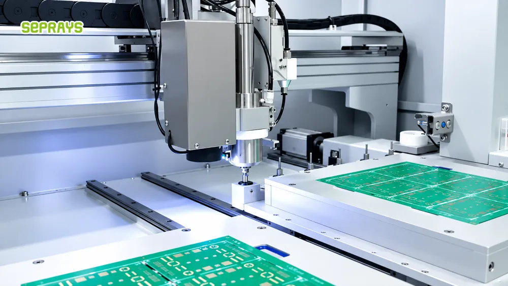
The GAM330 supports optional upper or lower dust collection configurations. Seprays states that these options are designed to help keep the PCB surface and working area clean after depaneling.
However, extraction should still be evaluated with the actual PCB.
Different materials and cutting conditions generate different amounts of debris.
A larger dust collector is not automatically the complete answer.
The extraction position, airflow, filter maintenance, cutter condition, and cutting parameters all matter.
💰 Looking at the Cost Beyond the Machine
For a smartphone-related production line, machine price is only one part of the calculation.
A more realistic model is:
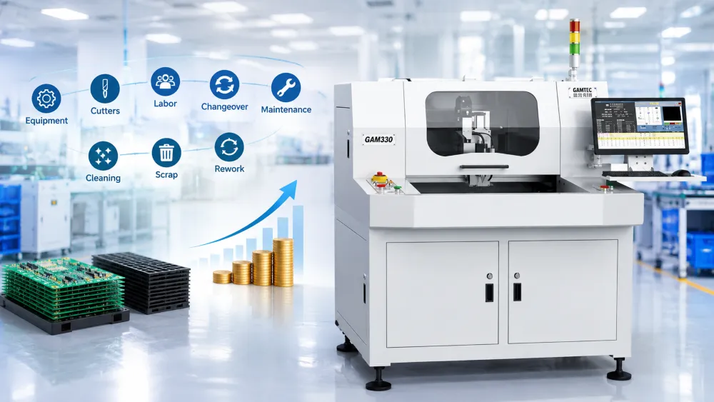
Equipment + cutters + labor + changeover + maintenance + cleaning + scrap + rework
Consider manual handling.
If an operator spends only several seconds positioning and unloading each panel, the number looks small.
Multiply that by thousands of cycles.
Now the number matters.
But there is another cost that is easier to miss:
quality-related cost.
If inconsistent separation creates additional inspection or rework, the production cost increases even when the machine itself is inexpensive.
This is why a stable process can sometimes be more valuable than a faster process.
🧪 A Real-World Seprays Application
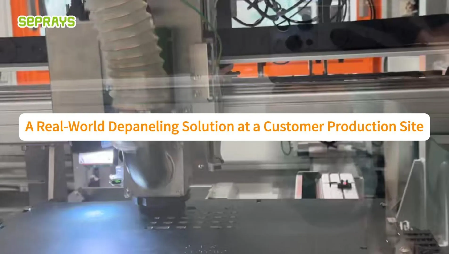
For a semiconductor-related electronics manufacturer serving the smartphone supply chain, Seprays Group approached the application from the production process rather than simply matching a machine specification.
The engineering evaluation considered the PCB outline, board size, cutting path, component clearance, production volume, operator workflow, and dust management.
The GAM330 was configured around the actual production requirements.
The goal was straightforward:
make PCB separation repeatable enough to fit the production process, not just demonstrate a good result on one sample.
The customer could then evaluate the complete cycle:
Panel loading → CCD positioning → programmed routing → board separation → dust collection → unloading
That sequence is more meaningful than looking at cutting speed alone.
📊 What the Production Team Should Measure
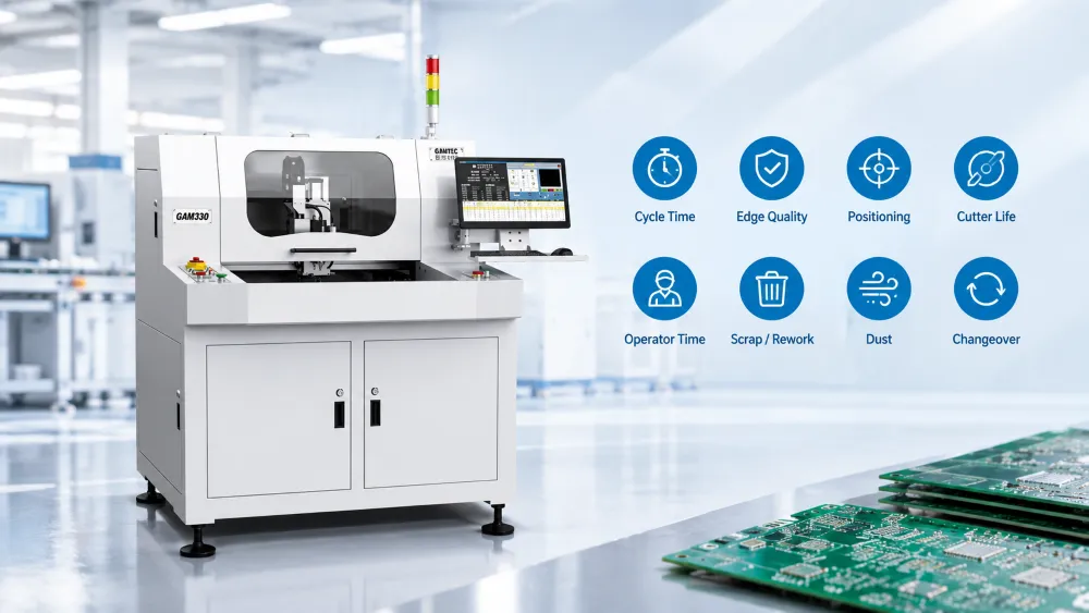
Before and after automation, several indicators can be compared:
| Production Indicator | What to Watch |
|---|---|
| Cycle time | Actual complete cycle, not cutting time only |
| Edge quality | Burrs, roughness, visible damage |
| Positioning | Repeatability between panels |
| Cutter life | Usage and replacement frequency |
| Operator time | Loading, unloading and adjustments |
| Scrap/rework | Boards requiring additional inspection |
| Dust | Cleaning frequency and extraction performance |
| Changeover | Time between PCB models |
This creates a more objective basis for equipment evaluation.
It also makes the results easier to verify internally.
🧠 The Counterintuitive Conclusion
For high-volume smartphone PCB production, the fastest cutter is not necessarily the most productive solution.
Why?
Because production is a system.
If cutting takes 20 seconds but loading takes 15 seconds, and unloading takes another 15 seconds, improving cutting speed alone may have limited impact.
A better result can sometimes come from reducing the waiting and handling around the cutting operation.
That is the lesson worth taking from this application:
Optimize the complete production cycle, not one number on the machine specification sheet.
🌎 Why Choose Seprays Group?
With more than 30 years of experience, Seprays Group has been dedicated to PCB/FPC depaneling technology, providing a full range of solutions—including milling-cutter depanelers, laser depanelers, V-Groove depanelers, punching depanelers, and automated handling systems.
Our equipment is trusted by leading manufacturers, including Foxconn, Flextronics, State Grid, Luxshare, Compal, Wistron, China Electronics, Quanta, CRRC, China Aerospace, OPPO, ZTE, and Bosch. Our equipment and solutions are used in factories across China and manufacturing facilities worldwide.
With more than three decades of experience, Seprays Group has worked with different PCB structures, production volumes, automation requirements, and depaneling processes.
For smartphone-related PCB production, this experience is particularly relevant because the separation process needs to work together with upstream loading, positioning, downstream handling, dust management, and production quality requirements.
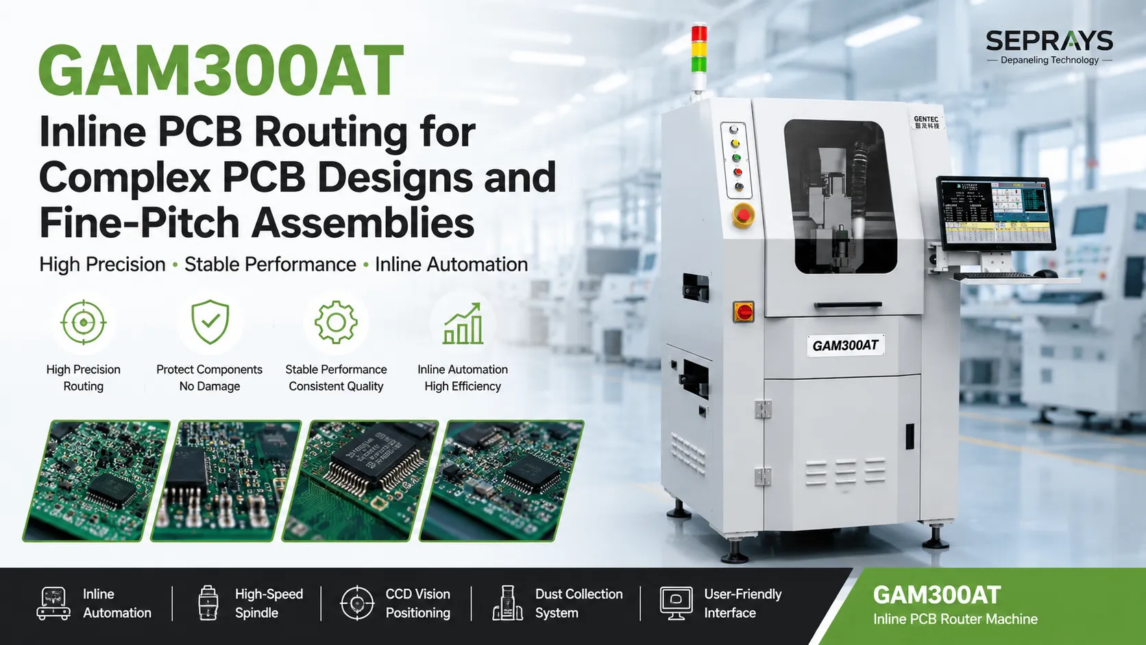
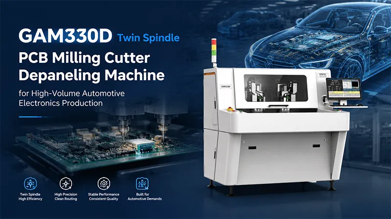
The GAM330 Automatic PCB Router Machine is designed for applications including small multi-connected boards used in mobile-phone electronics, as well as automotive electronics and other PCB applications. Its current configuration includes CCD automatic calibration, dual worktables, automatic tool changing, tool detection, and optional dust collection and MES integration.
For the right application, the starting point should be the actual PCB rather than the machine catalog.
A Gerber file, PCB drawing, panel layout, board thickness, production volume, and current depaneling process can help determine whether routing is appropriate.
If you have a similar PCB depaneling challenge, please contact us to discuss your application.
WhatsApp: +8618929266433
E-mail: sales@seprays.com
❓ FAQ
1. What type of smartphone PCB is suitable for routing?
Routing is suitable for small, multi-connected boards and PCB designs with irregular contours or programmed cutting paths. The actual suitability depends on board material, thickness, component clearance, and required edge quality.
2. Can the GAM330 handle different smartphone PCB designs?
The GAM330 supports programmable cutting paths and CCD-based positioning. Different PCB designs can therefore be evaluated and programmed according to their individual contours and production requirements.
3. How accurate is the GAM330?
The current product specifications list ±0.01 mm repeat precision and ±0.05 mm cutting precision. Actual production performance should still be verified using the customer’s PCB, tooling, fixture, and process parameters.
4. Does the GAM330 support automatic tool changing?
Yes. The machine uses an automatic tool-change spindle and also provides milling-tool detection functions to help manage cutter condition during production.
5. What should a smartphone PCB manufacturer provide for a machine evaluation?
The most useful information includes the PCB or Gerber file, panel layout, board thickness and material, component clearance, required edge quality, production volume, current separation method, and expected automation level. A sample test with the actual PCB is the best way to validate the final process.