.png)
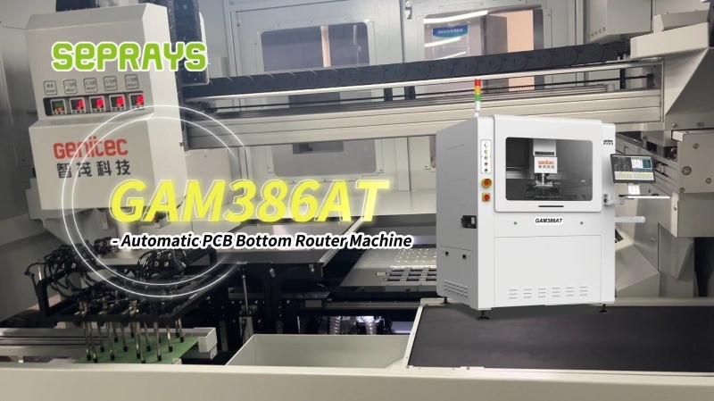
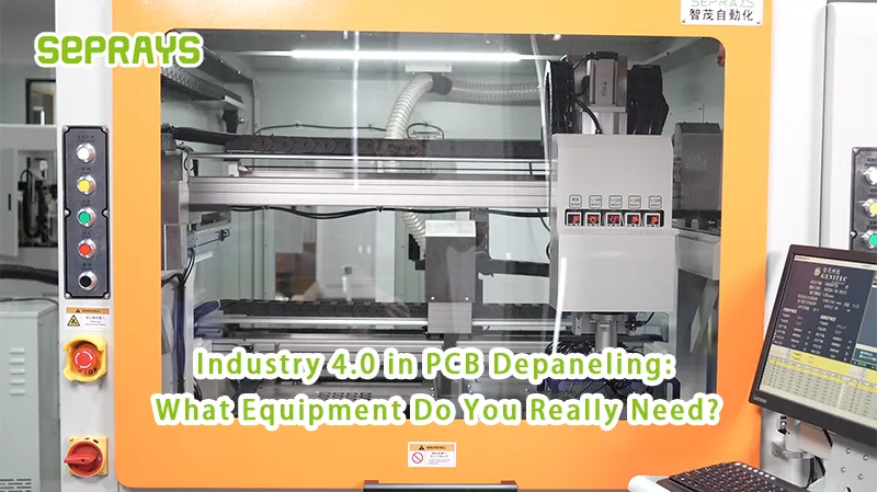
Automatic PCB Bottom Router Machine technology has become a core process in PCB depaneling for factories dealing with dense component layouts, fragile materials, and increasingly complex structures. A recurring question among European production engineers is straightforward but critical:
How can we guarantee that components are not damaged during high-speed routing?
Across different SMT lines in Germany and France, technicians share similar pain points — vibration affecting tall components, micro-cracks forming under thermal or mechanical stress, and unpredictable panel movement during cutting. Below is a collection of field-tested insights from daily production.

🔧 H1 — The Real Challenges Behind Component Safety in Bottom Routing
Damage rarely occurs “suddenly.” Instead, it results from small, accumulated mechanical forces. The most common factors include:
- Vibration transfer from the router bit to the PCB surface
- Operator-dependent clamping pressure when fixtures are used
- Panel bending caused by uneven material thickness
- Cutting load peaks when routing tight corners or thick copper areas
Engineers in high-reliability industries (e.g., automotive, industrial controls, aerospace) emphasize that even a 0.1–0.2 mm deflection can cause hidden cracking around sensitive components such as ceramic capacitors.
A bottom-routing approach reduces these issues by isolating cutting forces away from top-side components.
⚙️ H2 — Cost Analysis: The Hidden Financial Impact of Component Damage
Component damage doesn’t always show up immediately. Many plants report long-term costs that appear later in the product lifecycle:
- Warranty claims due to latent cracks or solder joint failure
- Rework fees when AOI or ICT detects instability
- Yield loss occurs when mechanical stress slightly shifts component positions
- Extra time spent tuning fixtures for each new PCB version
A German EMS provider noted that one cracked MLCC per panel increased annual scrap cost by over €40,000. This indicates that cutting stability has a direct impact on financial outcomes.
🧠 H3 — Case Study: Protecting High-Profile Components in Industrial Controllers
A French factory producing industrial automation modules had a recurring problem: tall components near routing edges experienced solder joint fatigue. Their conditions:
- 4-mm height connectors
- 1.0-mm thick FR-4
- Strong copper distribution asymmetry
- Annual volume: 900,000 units
Switching to a bottom router helped eliminate the majority of vibration reaching the top side. Combined with vision correction and soft support pads, their component damage rate dropped from 1.4% to 0.2%.
The key was controlling mechanical load distribution, not simply increasing spindle speed.
🛠️ H4 — Practical Solutions to Protect Components During PCB Bottom Routing
Below are proven engineering methods consistently found in European factories:
1. CCD Vision Correction for Position Accuracy
Distorted or slightly warped panels cause misalignment, which often leads to unexpected pressure around components. Vision correction minimizes these tolerances and stabilizes routing depth.
2. Soft and Distributed Support Instead of Hard Fixtures
Many German plants avoid rigid clamping to prevent stress points. Soft distributed support gently holds the PCB to maintain flatness without compressing components.
3. Optimize Routing Sequence
Cutting perimeter contours last maintains structural integrity for a longer period. Inner slots, which generate less movement, are processed earlier.
4. Use High-Precision Spindle Control
A stable high-speed spindle reduces load ripple, preventing vibrations from transmitting upward into the component side.
5. Bottom-Up Cutting Direction
This method isolates cutting forces away from the populated top layer, minimizing mechanical interaction with sensitive parts.
6. Edge Clearance and Copper Balancing
If designers leave insufficient clearance, routing forces concentrate near components. Collaboration between production and design teams is essential for continuous improvement.
🧩 H5 — Discussion: When Does an Automatic PCB Bottom Router Machine Become Necessary?
Based on shared feedback, bottom routing becomes critical when:
- Components sit less than 2–3 mm from routing edges
- Panels include fragile ceramics, connectors, inductors, or large ICs
- PCB thickness is ≤ 0.8 mm, increasing flex risk
- Warping or copper imbalance causes unpredictable mechanical stress
- Changeovers are frequent, and fixture costs grow over time
Engineers who adopt bottom routing typically do so to improve long-term reliability, not just to increase cutting speed.

⭐ Why Choose Seprays Group?
Seprays Group develops industrial-grade PCB depaneling solutions designed for factories facing real-world challenges such as component fragility, thin materials, and complex PCB layouts. Our bottom-routing systems focus on stability, durability, vision accuracy, and controlled cutting forces to help you reduce hidden failure risks and maintain consistent product quality.
If you need engineering advice or want to evaluate your current depaneling process, please contact us anytime.
WhatsApp: +8618929266433
E-mail: sales@seprays.com