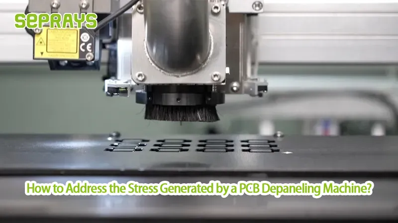
How Tooling, Spindle Speed, and Routing Paths Impact PCB Milling Cutting Effect is a topic frequently discussed among manufacturing engineers aiming to improve precision while controlling operational cost. Across German and French factories—known for their industrial craftsmanship, durability expectations, and engineering discipline—PCB milling performance is not judged only by cutting quality, but also by the long-term stability of the process.
In this article, we share practical insights from real factory experiences, cost analyses, and lessons learned from high-volume SMT lines.
🔧 H1: The Critical Role of Tooling Quality in Milling Performance
For many factories, tooling is often treated as a consumable rather than a strategic factor. However, engineers from automotive, aerospace, and telecom plants in the EU have repeatedly shown that:
- Tool geometry determines stress levels on PCBs
- Coating quality affects burr formation and heat resistance
- Shank precision influences vibration and cutting accuracy
When low-grade tools are used, micro-cracks, fiber tearing, and inconsistent edge profiles become common issues. Over time, this increases rework, tightens inspection tolerances, and raises operational cost.
Practical Factory Insight:
In one French EMS line, switching from standard carbide to coated micro-grain tooling extended tool life by 42% and reduced board-edge polishing time to nearly zero.

⚙️ H2: How Spindle Speed Affects Cutting Stability and Accuracy
High spindle speed is often assumed to deliver better cutting results—but this is not always true.
Key Relationships
- Too high: increases heat, accelerates tool wear, may burn materials
- Too low: causes chipping, rough edges, fiber pull-up
- Imbalanced speed: generates vibration that impacts routing repeatability
A stable German-style approach focuses on matching spindle speed to board material, not maximizing RPM. PCB thickness, copper density, and fiberglass hardness each require different cutting physics.
Case Example:
A Southeast Asian plant operating 24/7 found that reducing spindle speed by 8% improved dimensional stability because vibration dropped significantly.
📐 H3: Why Routing Path Planning Determines Cutting Efficiency
Routing paths determine:
- Cutting stress distribution
- Tool engagement time
- Heat accumulation
- Residual stress on components
Factories with high defect visibility (automotive, medical electronics) often use progressive routing—starting from the internal areas and moving outward—to minimize warpage and stress concentration.
Common Path Errors
- Sharp corners → micro cracks
- Single-pass deep cutting → heat deformation
- Irregular tab distribution → uneven stress release
Better Engineering Approach
Germany and France often adopt multi-pass routing, consistent tab spacing, and optimized lead-in angles to achieve durable, repeatable results.
📊 H4: Cost Analysis — How These Three Factors Influence Total Operational Expense
A balanced cutting process minimizes:
- Tool breakage
- Scrapped PCBs
- Spindle maintenance
- Inspection load
- Machine downtime
Small factories frequently underestimate indirect costs. For example:
| Factor | Cost Impact |
|---|---|
| Poor tooling | Higher scrap rate |
| Wrong spindle speed | Frequent tool change |
| Inefficient routing path | Longer cycle time |
When optimized together, PCB milling cost per panel can drop by 20–35%, especially in high-mix production lines.
🏭 H5: Real-World Improvement Case from a European EMS Plant
A mid-sized plant producing EV control boards implemented the following:
- Upgraded to coated carbide tools
- Reduced spindle speed by 5–12% based on the material
- Switched to multi-stage routing paths
Result:
Cutting accuracy improved from ±0.1 mm to ±0.05 mm, and tool life doubled—without purchasing new equipment.

🌍 Why Choose Seprays Group?
Seprays specializes in precision PCB depaneling technology, built with industrial-grade durability aligned with German and French engineering standards. Our strength lies in:
- Stable high-speed spindle architecture
- Advanced routing path algorithms
- Long-life tooling management
- Proven performance in automotive, LED, telecom, and medical industries
If you have questions or need tailored advice for your production line, please contact us anytime.
WhatsApp: +8618929266433
E-mail: sales@seprays.com
.png)


