.png)

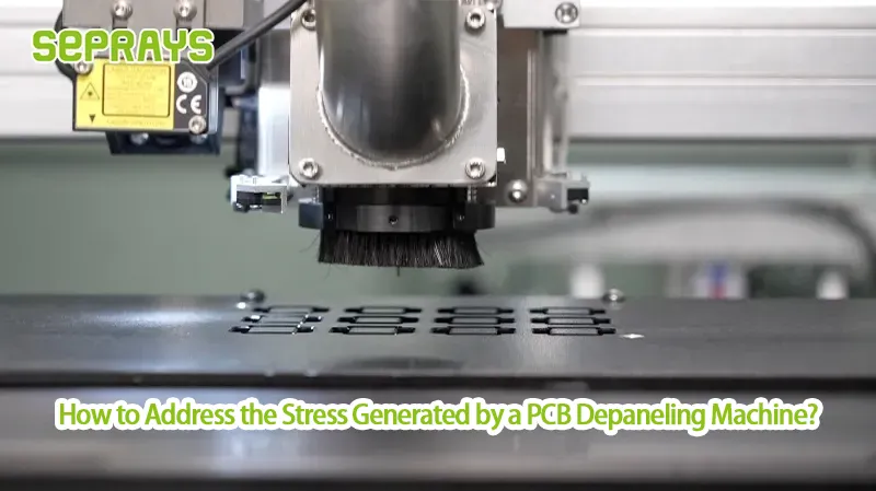
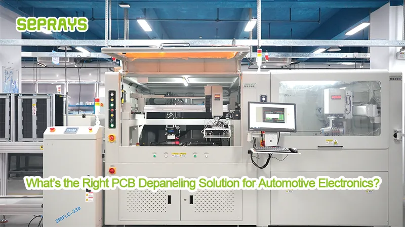
PCB depaneling remains a critical step in modern electronics manufacturing. PCB depaneling issues, such as cracks, delamination, or stress-induced warping, can disrupt production schedules, increase scrap rates, and drive up costs. Traditional depaneling methods—like mechanical routing or punching—often struggle with these challenges, especially when dealing with high-density boards or delicate components. This is where laser depaneling machines come in, offering precision, speed, and reliability.

✨ Understanding PCB Depaneling Challenges
Depaneling is more than just cutting boards into manageable sizes. It involves maintaining component integrity and ensuring that electrical connections remain intact. Common challenges include:
- Cracks around vias or sensitive components.
- Delamination of multilayer PCBs due to mechanical stress.
- Micro-fractures in boards with uneven thickness.
- High labor costs when using manual or semi-automatic methods.
Many manufacturers underestimate the impact of these issues until they notice increased board failure rates during functional testing. By addressing these pain points upfront, companies can save significant time and resources.
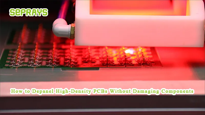
⚙️ How Laser Depaneling Machines Solve Cracks and Stress
Laser depaneling machines use focused laser beams to precisely cut PCBs without physical contact. This approach minimizes mechanical stress and heat damage. Key benefits include:
- Non-contact processing – No mechanical force is applied to the PCB, preventing cracks or stress.
- High precision – Lasers can cut complex shapes, including tight corners and intricate patterns, ideal for modern high-density PCBs.
- Consistency – Each board is cut with identical quality, reducing rework and scrap rates.
- Reduced downtime – Minimal fixture requirements and automated loading/unloading speed up production.
- Versatility – Compatible with a wide range of PCB materials and thicknesses.
By integrating laser depaneling, manufacturers can maintain high yield rates even on challenging boards, ensuring both quality and efficiency.
💡 Cost and ROI Analysis
Many companies hesitate to adopt laser depaneling due to perceived upfront costs. However, a closer look at the total cost of ownership (TCO) reveals the long-term benefits:
| Cost Factor | Traditional Depaneling | Laser Depaneling |
|---|---|---|
| Scrap Rate | 3-8% | <1% |
| Labor Costs | High (manual setup, supervision) | Low (automated) |
| Fixture Cost | High (custom jigs per board type) | Minimal |
| Maintenance | High (tool wear, replacement) | Low (minimal moving parts) |
| Downtime | Moderate | Minimal |
Investing in laser depaneling reduces rework, improves board integrity, and ultimately saves more money than it costs within the first few production cycles.
🏭 Real-World Case Studies
Case Study 1: High-Density Automotive PCB
An automotive electronics manufacturer faced repeated micro-cracks during mechanical depaneling. After switching to laser depaneling, defect rates dropped from 5% to 0.5%, while cycle time improved by 25%.
Case Study 2: IoT Device PCB Production
A company producing compact IoT devices struggled with delicate SMD components breaking during routing. Laser depaneling allowed precise, stress-free cuts, resulting in zero damaged components over a six-month production period.
Case Study 3: Prototype PCB Manufacturing
For prototype boards with variable thickness, laser depaneling eliminated the need for multiple fixtures. This flexibility saved both time and tooling costs, enabling faster product iteration.
🔍 Best Practices for Implementing Laser Depaneling
- Evaluate PCB material compatibility before installation.
- Optimize laser parameters (speed, power, focus) for minimal thermal impact.
- Integrate automated loading/unloading systems to maximize throughput.
- Regularly clean optical components to maintain cutting precision.
- Train operators on software and safety procedures for consistent results.
By following these guidelines, manufacturers can fully leverage laser depaneling benefits and maintain high-quality production standards.
💬 Encouraging Industry Discussion
The transition from mechanical to laser depaneling represents more than just an equipment change—it’s a step toward intelligent, flexible PCB manufacturing. Sharing experiences and challenges within professional forums or LinkedIn groups can help the industry evolve collectively. What strategies have you used to reduce depaneling stress? Are there specific board types that benefit most from laser depaneling in your experience?
✅ Why Choose Seprays Group?
Since 1993, Seprays Group has been dedicated to PCB/FPC depaneling technology, providing a full range of solutions — milling cutter depanelers, laser depanelers, V-groove depanelers, punching depanelers, and automated handling systems. Our equipment is trusted by leading manufacturers, including Foxconn, Flextronics, State Grid, Luxshare, Compal, Wistron, China Electronics, Quanta, CRRC, China Aerospace, OPPO, ZTE, and Bosch, serving factories across China and worldwide.
- CE-certified equipment with patented dust control designs.
- Global service network in 31+ countries.
- ISO9001, ISO14001, and ISO45001 certified.
- Over 32 years of manufacturing experience.
If you’re ready to upgrade your PCB depaneling process or have questions about the best solution for your production line, contact us today. Our team provides professional guidance and customized solutions to fit your needs.
📩 For more information, please contact us:
📱 WhatsApp: +86 189 2926 6433
📧 E-mail: sales@seprays.com