.png)
V-cut depaneling is fast, simple, and cost-effective—but it is not a universal solution. In real SMT production, many quality issues appear not because V-cut is “bad,” but because it is used in the wrong situations.
This article focuses on where V-cut starts to fail, based on production experience rather than theory.
⚠️ The Core Limitation of V-Cut Depaneling
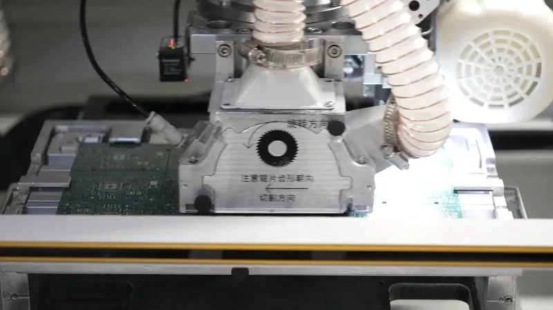
V-cut depaneling works by applying mechanical force along a pre-scored groove.
That means:
- Stress is unavoidable
- Force is transferred through the PCB
- The board must flex to separate
When boards or components cannot tolerate that stress, V-cut becomes risky.
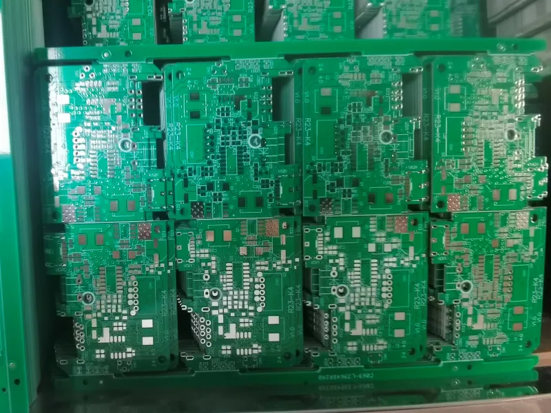
🧩 High-Density PCBA: A Common Problem Area
V-cut is not recommended when components are placed close to the board edge.
Typical risk scenarios:
- Fine-pitch ICs near the V-groove
- Ceramic capacitors (MLCCs) close to edges
- BGAs or QFNs on thin boards
In these cases, depaneling stress can cause:
- Micro-cracks in solder joints
- Latent failures after thermal cycling
- Yield loss that is hard to trace back
These issues often appear weeks later, not during depaneling.
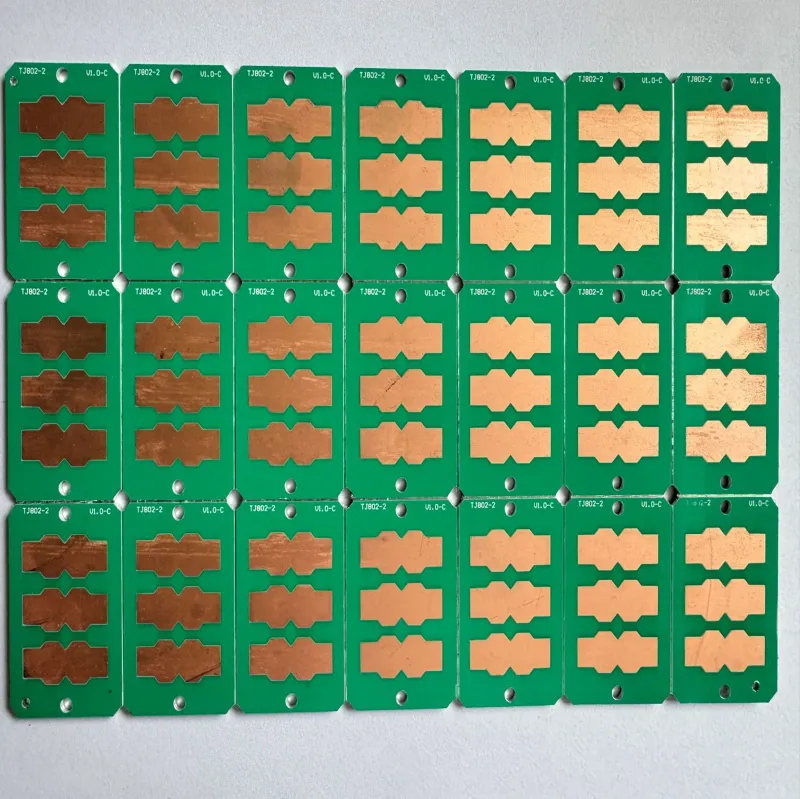
📉 Thin or Flexible PCBs
Thin PCBs (≤1.0 mm) and flexible or rigid-flex boards are poor candidates for V-cut.
Why?
- Thin boards bend more under force
- Stress spreads unevenly
- Edge breakout becomes harder to control
Even if separation “looks fine,” internal damage may already exist.
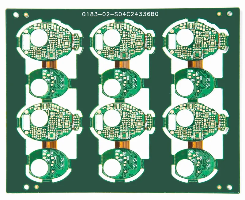
🔍 Irregular Board Shapes and Internal Cutouts
V-cut requires straight, continuous lines.
It is not suitable for:
- Curved outlines
- Internal slots or cutouts
- Step-shaped or non-rectangular boards
Trying to adapt V-cut to these designs usually leads to:
- Manual breaking
- Secondary trimming
- Inconsistent edge quality
At that point, the speed advantage disappears.
💥 Applications with High Reliability Requirements
V-cut depaneling is often avoided in:
- Automotive electronics
- Medical devices
- Industrial control systems
- Power electronics
In these industries, latent stress damage is unacceptable, even if immediate yield looks good.
Reliability standards often push manufacturers toward low-stress depaneling methods instead.
💰 Cost Analysis: Cheap Upfront, Expensive Later
V-cut systems have:
- Low machine cost
- High throughput
- Simple operation
But potential hidden costs include:
- Increased failure rates in field returns
- More inspection and testing
- Warranty or recall risks
For high-value PCBAs, these downstream costs often outweigh the initial savings.
🧪 A Real-World Example from the Shop Floor
In a consumer-industrial hybrid project supported by Seprays Group, a customer initially chose V-cut depaneling to maximize throughput.
As production ramped up:
- Field failures increased
- X-ray analysis showed solder joint cracking
- Failures correlated with boards depaneled by V-cut
After switching sensitive products to router depaneling while keeping V-cut for robust boards, yield stabilized, and complaint rates dropped.
The key takeaway: V-cut wasn’t wrong—the application was.
🔄 When to Consider Alternatives Instead
You should consider router or laser depaneling when:
- Components are within a few millimeters of the edge
- Board thickness is low
- Reliability is more important than speed
- Board shapes are complex
- Product value is high
In many factories, a mixed depaneling strategy works best.
💬 The Real Question to Ask
Instead of asking
“Is V-cut good or bad?”
Ask:
- How much stress can this PCBA tolerate?
- What is the cost of a hidden failure?
- Is speed more important than long-term reliability?
The right depaneling method depends on product risk, not habit.
⭐ Why Choose Seprays Group?
Seprays Group helps manufacturers evaluate when V-cut makes sense—and when it doesn’t. With experience across router, V-cut, and laser depaneling systems, Seprays focuses on matching the process to real production risks, not just cycle time.
If you are unsure whether V-cut depaneling is suitable for your boards, don’t hesitate to get in touch with us for a practical, engineering-level discussion.
WhatsApp: +8618929266433
Eメール: sales@seprays.com