.png)

PCB depaneling processes are critical in electronics manufacturing. Yet, many companies still rely on outdated or manual methods. These methods create bottlenecks, reduce yield, and increase production costs. So, what’s really holding back your production line, and how can smarter depaneling solutions help?
⚡ The Hidden Bottleneck in Production
Manual or semi-automatic PCB depaneling processes can’t keep pace with modern SMT lines.
Issues often include:
- Slow cutting speed
- High stress on components
- Inconsistent accuracy
When every second counts, these inefficiencies add up. The result is wasted time, higher labor costs, and delayed deliveries.

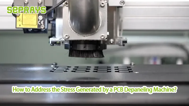
🔧 Stress and Damage: The Silent Profit Killers
Traditional depaneling often puts mechanical stress on PCBs. This leads to:
- Micro-cracks in solder joints
- Component misalignment
- Increased failure rates in the field
Modern PCB depaneling processes are designed to minimize stress. Less stress means stronger, more reliable boards and fewer warranty claims.
📊 Yield Matters More Than Speed Alone
Speed is important. But yield is critical.
Even a fast process is useless if it damages 5–10% of your boards.
Advanced depaneling machines use precision tools, vision systems, and intelligent software. Together, they ensure smooth, burr-free edges with minimal scrap. This balance of speed and accuracy boosts both throughput and profitability.
🌍 Automation: The Key to Scaling Production
As demand grows, manual PCB depaneling processes simply can’t scale.
Fully automatic machines offer:
- Inline integration with SMT lines
- Consistent quality 24/7
- Reduced reliance on skilled labor
This automation not only saves time but also frees operators to focus on higher-value tasks.
🛡️ Dust and ESD Protection for Reliability
A major risk in outdated depaneling processes is dust and static.
Dust particles can contaminate boards, while ESD can destroy sensitive components.
Modern machines include:
- Built-in dust collection systems
- Advanced ESD protection
- Cleaner, safer working environments
Better reliability means fewer failures and happier end customers.
🚀 Turning Bottlenecks Into Growth
Upgrading PCB depaneling processes isn’t just about cutting boards. It’s about unlocking capacity, reducing costs, and increasing competitiveness.
Companies that invest in advanced depaneling solutions often see:
- Faster time-to-market
- Lower defect rates
- Higher overall equipment effectiveness (OEE)
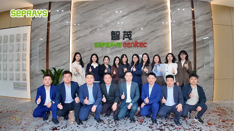
⭐ Why Choose Seprays Group?
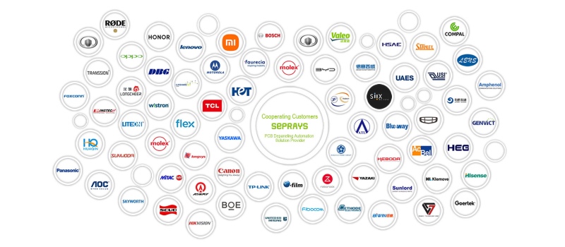
Since 1993, Seprays Group has been dedicated to PCB/FPC depaneling technology, providing a full range of solutions — milling cutter depanelers, laser depanelers, V-groove depanelers, punching depanelers, and automated handling systems. Our equipment is trusted by leading manufacturers, including Foxconn, Flextronics, State Grid, Luxshare, Compal, Wistron, China Electronics, Quanta, CRRC, China Aerospace, OPPO, ZTE, and Bosch, serving factories across China and worldwide.
- Over 32 years of manufacturing experience.
- CE-certified equipment with patented dust control designs.
- Global service network in 31+ countries.
- ISO9001, ISO14001, and ISO45001 certified.
With Seprays, you don’t just cut PCBs. You cut downtime, waste, and inefficiency.
📧 For more information, please contact us:
WhatsApp: +86 189 2926 6433
E-mail: sales@seprays.com