.png)
Laser PCB depaneling is often discussed when engineers start working with high-density PCBA designs. As boards become smaller and component spacing tighter, traditional mechanical separation methods sometimes reach their limits. Many production teams then begin evaluating laser cutting as an alternative.
But is laser depaneling always the best option for high-density PCBA? In practice, the answer depends on board layout, reliability requirements, and production strategy. Let’s look at the issue from a real manufacturing perspective.
🔍 Why High-Density PCBA Changes the Depaneling Challenge
High-density PCBA designs are very different from older PCB layouts. Components are packed closer together, and the space near the board edge becomes extremely limited.
Common characteristics include:
- components placed less than 1 mm from the edge
- thin or flexible PCB materials
- miniaturized modules for consumer electronics
- dense RF or communication circuits
In these situations, depaneling becomes more than just a separation step. It can directly affect component reliability and final product quality.
This is why engineers frequently revisit the question: Is laser PCB depaneling the right solution?
⚠️ The Mechanical Stress Problem
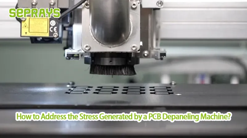
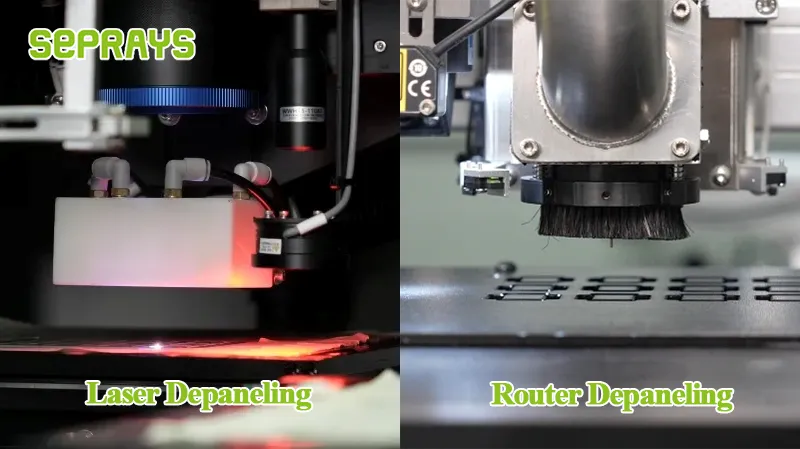
One challenge with mechanical depaneling methods is cutting force and vibration.
Processes such as router depaneling involve a rotating milling tool contacting the board. For many standard PCBs, this works perfectly fine. However, when boards become thin, or components sit very close to the edge, the cutting force can introduce risks like:
- Microcracks in MLCC capacitors
- Stress on solder joints
- Small board deformation
- Long-term reliability concerns
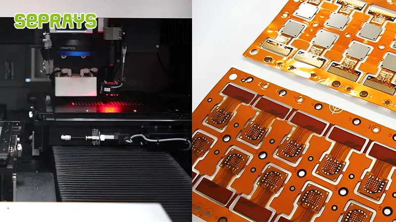
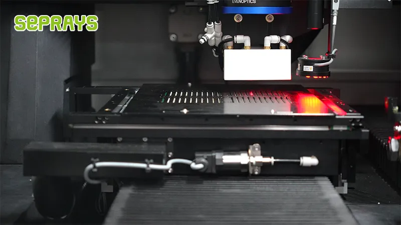
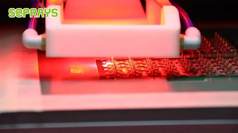
Laser depaneling removes this contact entirely. The board is separated using a focused beam rather than a physical tool.
📏 Precision Requirements in Modern Electronics
High-density PCBA often requires extremely precise cutting boundaries.
Laser depaneling offers several technical advantages:
- High precision cutting (<2 μm repeatability)
- No mechanical stress or vibration
- Very narrow kerf width (<25 μm)
- Clean edges without tool wear
The narrow cutting path also allows engineers to maximize PCB material utilization, which can help reduce material waste in high-volume production.
These characteristics make laser systems attractive for miniaturized electronic products.
📊 Laser vs Mechanical Depaneling Comparison
Engineers often evaluate depaneling options using simple production criteria.
| Factor | Mechanical Depaneling (Router) | 레이저 구분 |
|---|---|---|
| Cutting method | Physical milling tool | Focused laser beam |
| Mechanical stress | 당 | None |
| 정밀 | Good | Very high |
| Tool wear | Requires tool replacement | 없는 도구를 착용 |
| Edge clearance requirement | Larger | Smaller |
| Equipment investment | Lower | Higher |
Both technologies are valuable in modern manufacturing. The choice usually depends on design constraints and production priorities.
💰 Cost Considerations in Real Production
Laser depaneling machines typically require a higher initial investment. This is often the first concern raised by production managers.
However, the overall cost picture includes more factors:
- Tool replacement for milling cutters
- Machine maintenance
- Yield loss from component damage
- Production downtime
For high-density PCBA products with high unit value, the cost of potential defects may exceed the equipment price difference.
That is why many factories adopt laser depaneling specifically for sensitive product lines, while continuing to use mechanical methods for standard boards.
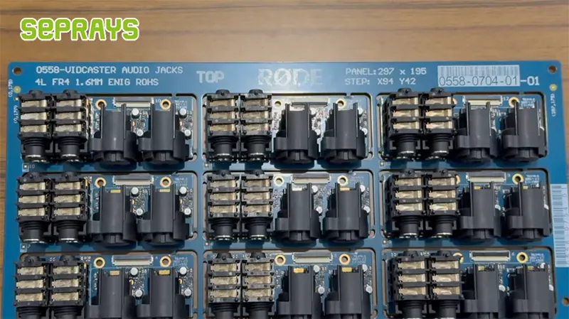
🏭 A Practical Case from Production
A manufacturer producing compact communication modules faced recurring reliability issues during final testing. The PCB design placed small capacitors very close to the board edge.
The production line originally used router depaneling. Although the process was stable, occasional component damage appeared during stress testing.
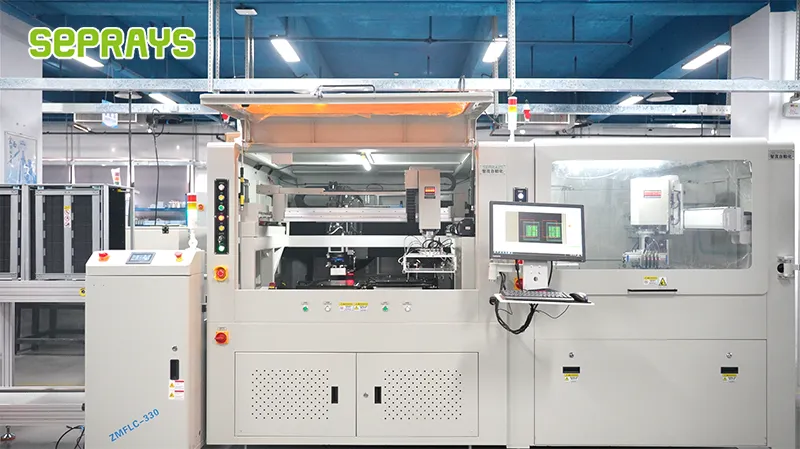
After reviewing the process, the engineering team evaluated a laser depaneling system supplied by Seprays Group for this particular product series.
After several months of production, they observed:
- Reduced component stress near the board edge
- Improved consistency of cutting quality
- More stable yield in high-volume runs
The company still uses router depaneling for larger boards, but laser systems are now used for high-density modules.
🧠 When Laser Depaneling Makes the Most Sense
Based on real production experience, laser PCB depaneling is often preferred when:
- Components are extremely close to the PCB edge
- Boards are thin or fragile
- Complex outlines require flexible cutting paths
- High product reliability is required
- High-density layouts limit mechanical separation
For conventional PCBs with enough edge clearance, mechanical depaneling methods can still provide excellent efficiency.
🔧 A Balanced Approach for Modern PCBA Manufacturing
Instead of choosing a single technology, many manufacturers adopt a hybrid depaneling strategy.
Typical setup:
- Router depaneling for standard boards
- Laser depaneling for high-density or sensitive PCBA
This approach allows factories to balance cost, efficiency, and reliability across different products.
Ultimately, the best method is the one that supports the specific design and production requirements of the PCB.
⭐ Why Choose Seprays Group?
Seprays Group focuses on PCB depaneling technologies used in modern electronics manufacturing. The company provides solutions such as:
- PCB router depaneling machines
- Laser depaneling systems
- Saw blade depaneling equipment
- Inline and offline depaneling automation
With experience across consumer electronics, industrial control systems, and automotive electronics, Seprays works closely with engineers to identify the most suitable depaneling method for each PCB design.
Since 1993, Seprays Group has specialized in PCB and FPC depaneling technologies, offering solutions including router depanelers, laser depanelers, V-groove depanelers, punching systems, and automation equipment. Our machines are used by manufacturers such as Foxconn, Flex, Luxshare, Compal, Wistron, Quanta, CRRC, OPPO, ZTE, and Bosch in production facilities worldwide.
If you are evaluating PCB depaneling solutions, please feel free to contact us for a technical discussion.
WhatsApp: +8618929266433
이메일: sales@seprays.com
❓ FAQ
1. Is laser PCB depaneling suitable for all PCB types?
Not always. Laser depaneling works best for high-density or delicate PCBs. For standard boards with enough edge clearance, router depaneling may be more cost-effective.
2. Does laser depaneling affect PCB materials?
Modern laser systems are designed to minimize thermal impact. With correct parameters, they can cut materials like FR-4, polyimide, and flexible PCBs with clean edges.
3. Is laser depaneling slower than router depaneling?
It depends on the board design and cutting path. For complex shapes or high-precision applications, laser cutting can be very efficient.
4. What industries commonly use laser PCB depaneling?
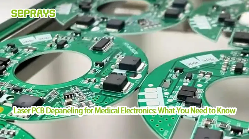
Consumer electronics, automotive electronics, medical devices, and communication modules frequently use laser depaneling due to their high-density PCB designs.
5. How do engineers decide between laser and mechanical depaneling?
Key factors include component distance from the board edge, PCB thickness, product reliability requirements, and production cost considerations.