.png)
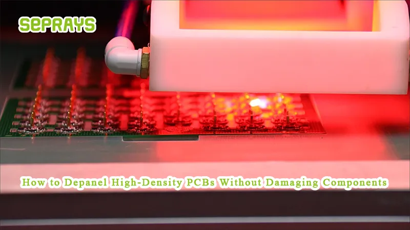
PCB Panel Cutting Machine performance becomes increasingly critical as modern electronics move toward thinner substrates and higher component density. In recent years, SMT engineers across Europe, North America, and Asia have shared similar challenges: maintaining cut accuracy without introducing stress, protecting fine-pitch components, and controlling long-term operating costs. This article summarizes practical lessons learned from real production environments rather than theoretical specifications.
🔬 Thin PCB Panels — Stability Before Speed
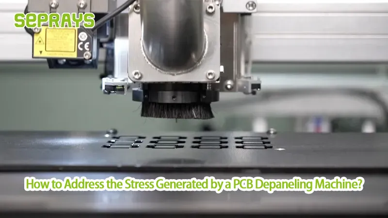
Thin PCB panels, often below 1.0 mm, behave very differently during depaneling. Engineers frequently report micro-vibration, panel flexing, and edge chipping as major risks.
Common pain points include:
- Deformation during mechanical cutting
- Stress transfer to nearby BGA and QFN components
- Difficulty maintaining consistent kerf width across large panels
In practice, factories mitigate these risks by prioritizing rigid support structures, controlled feed rates, and cutting paths designed to distribute stress evenly rather than maximize throughput.

🧠 High-Density Designs — Clearance Is the Real Constraint
High-density PCBs leave little margin for error. Component-to-edge distances continue to shrink, and traditional cutting assumptions no longer apply.
Observed challenges:
- Tool collision risks with tall or edge-mounted components
- Increased sensitivity to burrs and micro-cracks
- Greater dependence on accurate fiducial recognition
Many SMT lines now evaluate cutting machines based on vision accuracy, Z-axis repeatability, and tool control precision rather than raw cutting speed.

⚙️ Process Selection — Router, Laser, or Hybrid Approaches
No single cutting method fits all thin or dense PCB applications.
- Router cutting offers flexibility but requires excellent vibration control and dust management.
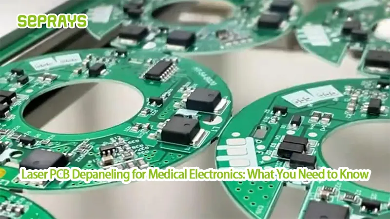
- Laser cutting minimizes mechanical stress and is often favored for ultra-thin or RF boards, though thermal behavior must be carefully managed.
- Hybrid strategies—using routing for outer contours and laser for sensitive areas—are increasingly discussed in advanced production lines.
The lesson shared by many engineers: process stability matters more than theoretical capability.

📉 Cost Analysis — Hidden Losses in Thin PCB Processing
While the machine price is often debated, experienced factories focus on indirect costs:
- Scrap caused by invisible micro-cracks
- Rework from edge damage discovered during testing
- Downtime from frequent tool changes or recalibration
- Yield loss traced back to depaneling-induced stress
In several cases, improving cutting stability reduced total production cost even when equipment investment increased slightly.
🏭 Case Observations from Global SMT Lines
- Germany: Automotive suppliers favor low-stress cutting methods to protect long-life electronics.
- United States: Mixed-product lines prioritize flexible routing systems with reliable vision correction.
- Asia: High-volume factories balance speed with panel support optimization to prevent warpage.
Despite regional differences, all cases point to one conclusion: thin and dense PCBs expose weaknesses quickly in poorly designed cutting systems.
🧩 Practical Engineering Guidelines
From shared workshop discussions, several consensus points emerge:
- Rigid panel support is non-negotiable
- Stress control outweighs maximum throughput
- Vision accuracy directly affects long-term yield
- Preventive maintenance defines real durability
- Cutting quality must be evaluated over months, not samples
These guidelines help engineers move from short-term testing toward sustainable production.
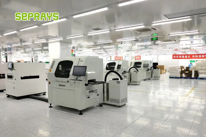
Why Choose Seprays Group?
Seprays Group designs PCB panel cutting solutions with a strong focus on industrial durability, process stability, and long-term precision—qualities essential for thin and high-density PCB applications. Our systems support multiple cutting technologies while emphasizing stress control and consistent quality over extended production cycles.
If you would like to discuss your specific PCB challenges or review cutting test results, please contact us.
WhatsApp: +8618929266433
E-mail: sales@seprays.com