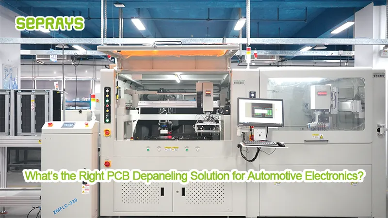
.png)
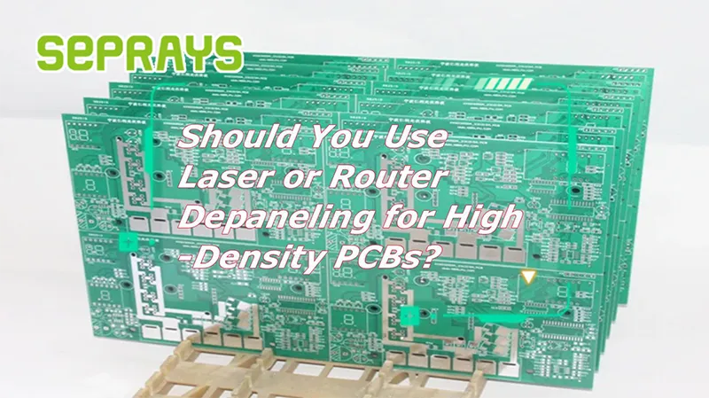
Laser or router depaneling for high-density PCBs? This question appears frequently when engineers design compact boards with tight component spacing. As PCBs become smaller and more complex, choosing the right depaneling method directly affects product reliability, yield rate, and long-term manufacturing cost.
Many teams initially choose based on equipment price alone. In practice, the real decision often comes down to board structure, component distance to edge, stress tolerance, and production scale.
🔍 The Core Question Behind Depaneling Choice
High-density PCBs usually place components close to the board edge. This makes mechanical stress during separation a critical concern.
Two common solutions exist:
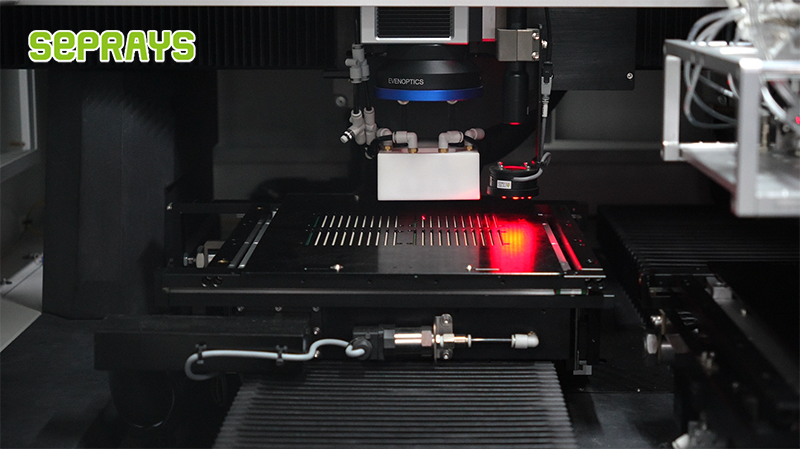
- Router depaneling – mechanical cutting with rotating tools
- Laser depaneling – non-contact cutting using focused laser energy
Both methods are widely used in electronics manufacturing. The key question is not which is better overall, but which fits your specific PCB design.
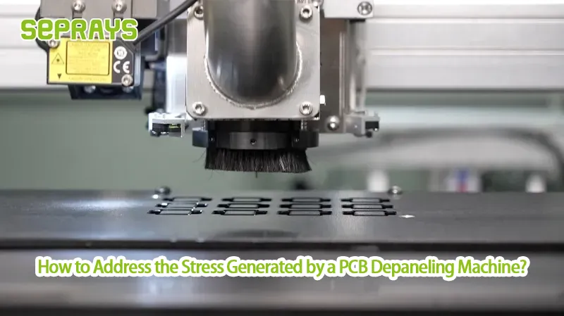
⚙️ Router Depaneling — Reliable and Cost-Effective
Router depaneling has been a standard process in the PCB industry for years. It works well for many production environments.
Typical advantages include:
- Lower equipment investment
- Mature and stable technology
- High throughput for many rigid PCBs
- Suitable for thicker boards
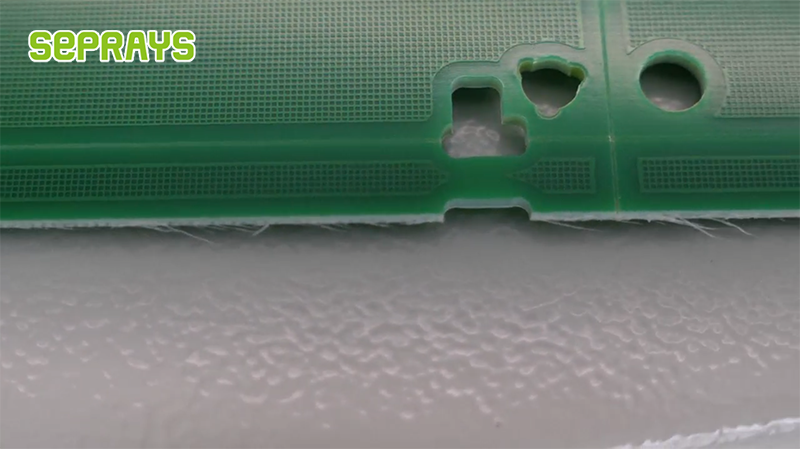
However, router cutting introduces mechanical vibration and cutting force. When components sit very close to the PCB edge, this stress can sometimes lead to:
- Micro-cracks in solder joints
- Ceramic capacitor damage
- Hidden reliability issues after assembly
For boards with larger edge clearance, router depaneling remains an efficient and practical option.
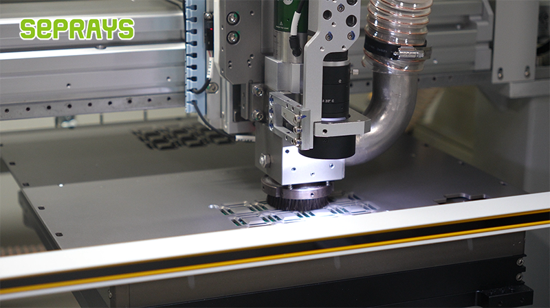
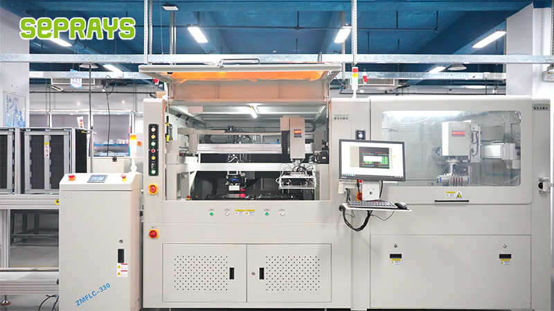
⚡ Laser Depaneling — Precision for Sensitive Designs
Laser depaneling uses a non-contact cutting process, meaning the PCB is separated without mechanical force.
This approach provides several advantages for high-density designs:
- Minimal mechanical stress
- Extremely narrow cutting path
- High precision for complex outlines
- Suitable for thin substrates and flexible boards
Because no physical tool touches the board, laser systems are often used for:
- RF modules
- Camera modules
- Medical electronics
- Wearable devices
The trade-off is typically a higher initial equipment cost and sometimes a slightly slower cutting speed, depending on material type.
💰 Cost Is More Than Equipment Price
A common mistake is evaluating depaneling methods purely based on machine cost.
In real production environments, several hidden costs matter:
- Yield loss from micro-cracks
- Component damage near board edges
- Rework or field failure risk
- Tool wear and maintenance
For high-density assemblies, reducing stress-related defects can significantly improve final product reliability. In some cases, the savings from higher yield offset the higher equipment investment.
🧩 A Real Production Scenario
One electronics manufacturer producing compact IoT modules faced recurring reliability issues. Components were placed within 0.5 mm of the PCB edge, and router cutting occasionally caused solder joint stress.
After evaluating alternatives, the team tested a laser depaneling solution from Seprays Group. The non-contact cutting process reduced mechanical impact on the board.
Within several months of production:
- Edge-related defects decreased noticeably
- Product reliability improved
- Process consistency became easier to control
The company still uses router depaneling for some standard products, but switched to laser for high-density modules where stress control is critical.
🧠 Practical Guidelines Engineers Often Use
Based on industry experience, engineers often consider these factors when selecting a depaneling method:
Choose router depaneling when:
- Component clearance from the edge is sufficient
- Boards are thick and rigid
- High throughput is the top priority
- Production cost must remain minimal
Choose laser depaneling when:
- Components sit extremely close to the edge
- Boards are thin or fragile
- Stress must be minimized
- Design complexity requires precise cutting
The best solution often involves using both technologies for different products.
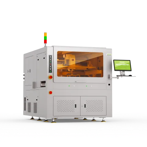
🚀 Why Choose Seprays Group?
Seprays Group focuses on PCB depaneling technology for modern electronics manufacturing. The company provides multiple solutions, including:
- Laser PCB depaneling systems
- Router depaneling machines
- Saw blade depaneling equipment
- Inline automation solutions
With experience supporting manufacturers across consumer electronics, automotive electronics, and industrial devices, Seprays aims to help engineers choose the most suitable process rather than simply selling equipment.
If you are evaluating depaneling solutions for high-density PCBs, feel free to contact us for discussion or technical support.
WhatsApp: +8618929266433
Электронная почта: sales@seprays.com