.png)
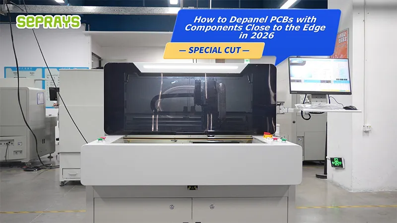
How to depanel PCBs with components close to the edge is one of those challenges that only shows up when designs get tighter—and in 2026, that’s almost every project.
You finish assembly.
Everything looks fine.
Then, the paneling happens.
And suddenly:
- Components crack
- Solder joints weaken
- Yield drops
The issue is not the PCB.
It’s the stress introduced during separation.
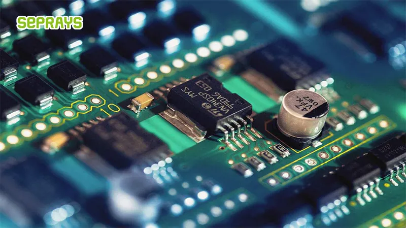
🔍 Why Edge-Proximate Components Are So Risky
Modern PCB designs push components closer to the edge to:
- Save space
- Reduce board size
- Optimize cost
But this creates a fragile zone.
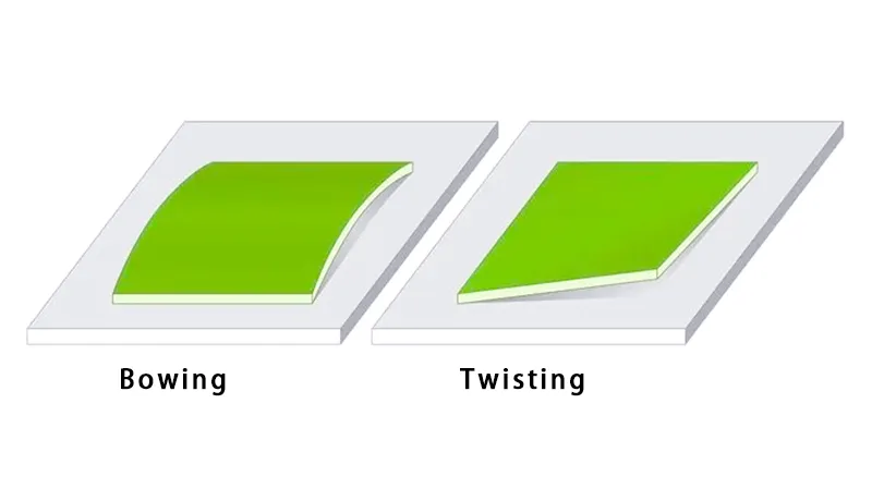
Even small mechanical stress can cause:
- MLCC cracking
- BGA solder fatigue
- Micro fractures in traces
The closer the component, the higher the risk.
⚙️ What Actually Causes the Damage
From real production experience, damage usually comes from:
1. Mechanical Stress
- Saw blade vibration
- V-cut breaking force
- Routing pressure
2. Improper Support
- PCB flex during cutting
- Lack of fixture stability
3. Tool and Parameter Mismatch
- Incorrect cutting speed
- Worn tools
- Poor path planning
💥 Common Mistakes Engineers Still Make
Even experienced teams fall into these traps:
- Using V-cut for sensitive edge components
- Applying manual braking for speed
- Ignoring tool wear
- Underestimating stress impact
These decisions often save time in the short term.
But it increases the cost long-term.
💡 A Counterintuitive Insight
You might think:
“Smaller cutting force is always safer.”
But that’s not always true.
- Too slow → increases heat and friction
- Too fast → increases vibration
The key is balance, not minimum force.
🧩 Best Depaneling Methods for Edge-Sensitive PCBs
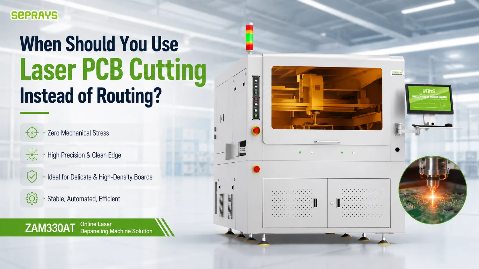
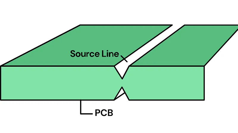
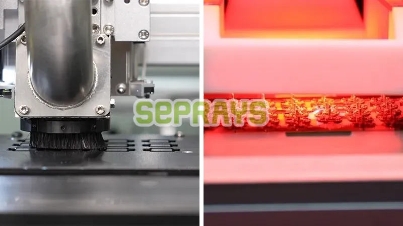
1. Laser Depaneling
Best for:
- Ultra-sensitive components
- High-density designs
Advantages:
- No mechanical stress
- High precision
Limitations:
- Higher cost
- Slower on thick boards
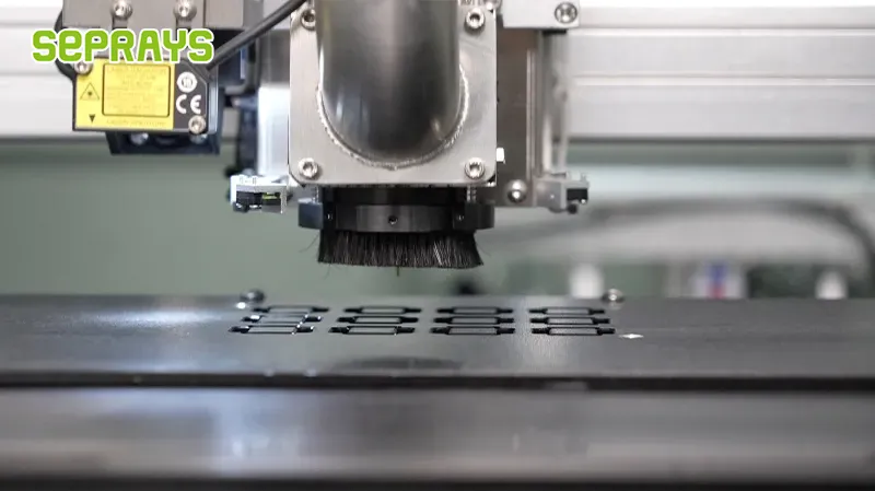
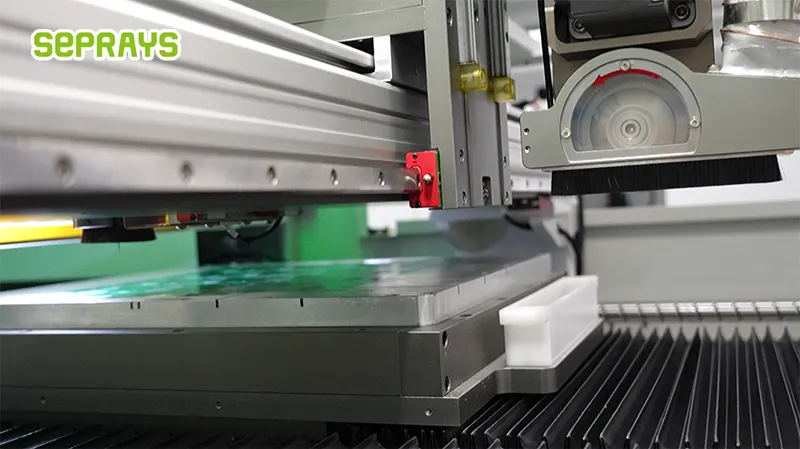
2. Router Depaneling (Optimized)
Best for:
- Complex shapes
- Moderate sensitivity
Advantages:
- Controlled cutting
- Good edge quality
Key condition:
- Proper fixture support
- Optimized tool path
3. Hybrid Approach
Best for:
- Mixed PCB structures
Example:
- Laser near sensitive areas
- Router for general cutting
📊 Method Comparison for Edge Components
| Method | Stress Level | 精密 | Efficiency | Best Scenario |
|---|---|---|---|---|
| Laser | Very Low | High | 介质 | Ultra-sensitive edges |
| Router | 介质 | High | 介质 | General complex boards |
| V-Cut | High | Low | High | Not recommended for edge components |
| Hybrid | Optimized | High | High | Mixed requirements |
🧪 Case Example — Preventing Edge Damage
A manufacturer producing compact IoT PCBs faced:
- Components within 0.5 mm of the board edge
- High failure rate after depaneling
- Cracked capacitors during testing
Initial method:
- V-cut separation
Problems:
- Excessive mechanical stress
- Hidden defects
After working with Seprays, they switched to:
- Laser depaneling for sensitive edges
- Optimized routing for other areas
Results:
- Significant reduction in component damage
- Improved product reliability
- Lower rework cost
The biggest improvement?
Damage prevention before it happens.
🛠️ Practical Solutions You Can Apply
From real production setups:
- Increase edge clearance if the design allows
- Use low-stress depaneling methods
- Add proper fixture support
- Optimize cutting parameters
- Regularly monitor tool condition
These are not complex changes.
But they are critical.
🔄 When Should You Upgrade Your Process?
Consider upgrading if:
- Components are within 1 mm of the edge
- You see unexplained field failures
- Defect rate increases after depaneling
- New designs reduce edge clearance
These are clear warning signs.
💰 Cost Perspective — Prevention vs Repair
Edge damage is expensive.
Not just in scrap.
But in:
- Warranty claims
- Customer dissatisfaction
- Brand reputation
Investing in the right depaneling method often costs less than fixing failures later.
🚀 Final Thought — Design and Process Must Match
PCB design is evolving.
Depaneling must evolve with it.
If components are closer to the edge,
your cutting method must be more precise.
There is no shortcut.
🚀 Why Choose Seprays Group?
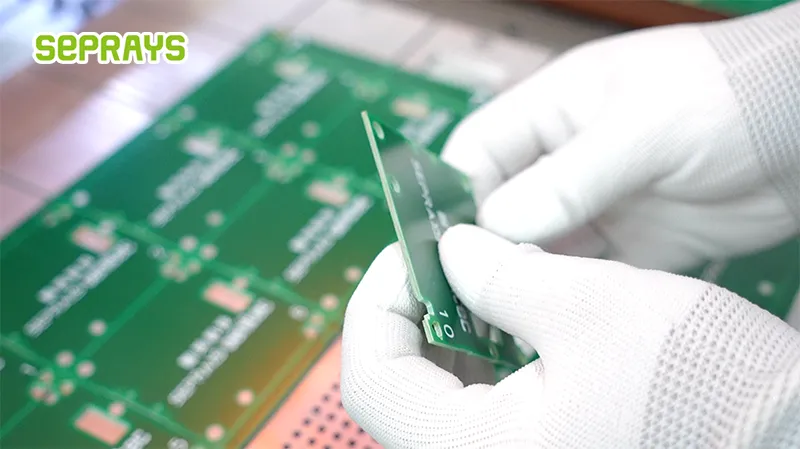
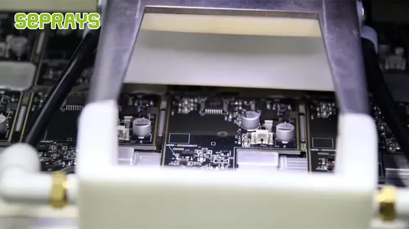
Seprays Group specializes in solving complex depaneling challenges, especially for high-density PCBs and edge-sensitive component layouts.
With over 30 years of experience, Seprays Group has been dedicated to PCB/FPC depaneling technology, providing a full range of solutions—milling-cutter, laser, V-groove, and punching depanelers, as well as automated handling systems. Leading manufacturers, including Foxconn, Flextronics, State Grid, Luxshare, Compal, Wistron, China Electronics, Quanta, CRRC, China Aerospace, OPPO, ZTE, and Bosch, trust our equipment. It is used in factories across China and worldwide.
With deep application expertise, Seprays helps customers reduce stress-related defects, improve yield, and ensure long-term product reliability.
If you are dealing with PCBs with components near the edge, feel free to contact us—we’re here to help.
WhatsApp: +8618929266433
❓ FAQ
1. Why are edge components easily damaged during depaneling?
Because they are exposed to mechanical stress during cutting.
2. Is V-cut suitable for edge-sensitive PCBs?
No, it generates high stress and is not recommended.
3. What is the safest depaneling method?
Laser depaneling offers the lowest stress.
4. Can routing be used safely?
Yes, with proper fixtures and optimized parameters.
5. How to reduce depaneling defects?
Choose the right method, optimize process settings, and ensure proper support.