.png)
 Chinese
  English
  Spanish
  Japanese
  Korean
  Russian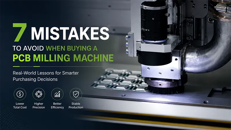
7 Mistakes to Avoid When Buying a PCB Milling Machine
Buying a PCB milling machine can look straightforward on paper. Compare cutting speed, working area, spindle power, price, and automation level. Pick the machine that appears to offer the most. In practice, that approach often leads to expensive surprises. A machine may be fast but poorly matched to the board design. A cheaper model may require more manual work. A highly automated system may be unnecessary for a factory running only a few hundred panels a day. The better question is not, “Which machine has the best specifications?” It is, “Which machine fits the way we actually produce PCBs?” Here are seven mistakes worth avoiding before making that decision. 🔎 1. Choosing the Machine Before Checking the PCB The first mistake is starting with the equipment instead of the board. PCB shape, thickness, material, component height, cutting path, panel size, and production volume all affect the process. A router-based solution is usually useful for irregular outlines and internal cutouts. But if your boards have long, straight V-grooves, another depaneling method may be more practical. Before requesting quotations, prepare: Practical lesson: send real samples whenever possible. A supplier’s standard test board cannot represent every production condition. ⚠️ 2. Looking Only at
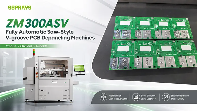
ZM300ASV Fully Automatic V-Groove PCB Depaneling for High-Volume Electronics Manufacturing
ZM300ASV fully automatic V-groove PCB depaneling becomes interesting when production volume grows, operators can no longer keep up, and a simple separation step starts affecting the whole SMT line. For a low-volume workshop, manually separating V-scored boards may still be perfectly reasonable. At higher volumes, the calculation changes. Labor consistency, cycle time, board handling, edge quality, and downstream automation become part of the real cost. That is where a fully automated approach deserves a closer look. 🔍 When Does V-Groove Separation Become a Production Problem? V-groove boards are attractive because the separation path is already defined. The process is relatively straightforward compared with routing complex PCB outlines. But “simple” does not always mean “easy to scale.” Imagine a production line running several shifts. Operators need to: A small inconsistency repeated hundreds or thousands of times can become a quality issue. For electronics manufacturers, the question is therefore not only “Can we separate the board?” It is “Can we separate every panel consistently without creating another bottleneck?” ⚙️ What Makes the ZM300ASV Different? The ZM300ASV is designed around this production-line problem rather than treating separation as a standalone manual operation. Its workflow can include automatic feeding, cutting, unloading, and waste collection.
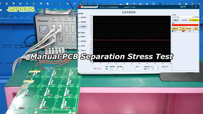
Manual PCB Separation Stress Test: How to Evaluate PCB Damage and Depaneling Risk
Manual PCB Separation Stress Test is a practical way to understand how much mechanical stress a PCB assembly can tolerate before choosing a production depaneling method. For engineers, the question is rarely just “Can this PCB be separated?” A better question is: What happens to the board and its components during separation, and can the same result be repeated thousands of times? This matters even more for high-density PCBA used in automotive electronics, medical devices, industrial controls, communication equipment, and semiconductor-related systems. 🔍 Why Perform a Separation Stress Test? A PCB can look perfectly normal after separation while still having problems that are difficult to see immediately. Potential risks include: A useful test should therefore examine the complete assembly, not only the cut edge. For example, a board with large component spacing may tolerate manual breaking or V-groove separation. The same method may become unsuitable when large components are positioned close to the separation line. The key variable is often where the stress goes, not simply how much force is applied. 🧪 How to Conduct a Practical Manual Stress Test A simple engineering test can provide useful information before investing in equipment. Step 1: Record the PCB Condition Document the
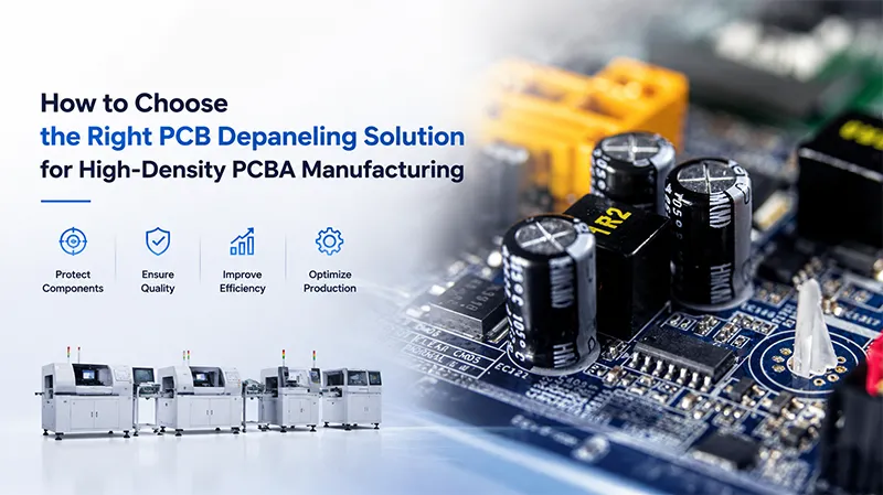
How to Choose the Right PCB Depaneling Solution for High-Density PCBA Manufacturing
Choosing the right PCB Depaneling Solution has become a more important decision for electronics manufacturers as PCBA designs continue to become smaller, denser, and more complex. Many engineers discover that the cutting process itself is not the biggest challenge. The real challenge is maintaining stable quality when production volume increases. For high-density PCBA manufacturing, factors such as component protection, process consistency, production efficiency, and future automation capability often determine whether a solution can support long-term manufacturing goals. A method that works well for prototype production may not always perform well in mass production. 🔍 Why High-Density PCBA Manufacturing Creates New Depaneling Challenges Modern electronic products are becoming more integrated. AI devices, automotive electronics, medical equipment, communication systems, and industrial controllers all require PCBs with: In these applications, PCB separation is no longer a simple mechanical process. A small amount of stress during cutting may affect: For example, a consumer electronics board with large spacing may tolerate a traditional separation method. However, a high-density control module with components close to the cutting path requires much stricter process control. This is why many manufacturers now evaluate depaneling equipment based on stability rather than only cutting speed. ⚠️ Common Problems with Traditional PCB
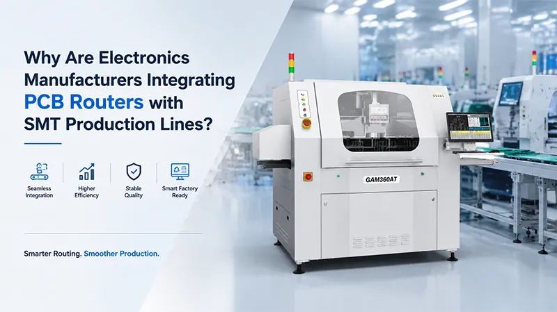
Why Are Electronics Manufacturers Integrating PCB Routers with SMT Production Lines?
PCB router integration with SMT production lines has become an important topic among electronics manufacturers looking to improve factory efficiency. In the past, many companies treated PCB routing as an independent finishing process. However, as electronics products become smaller, smarter, and produced in higher volumes, manufacturers are discovering a new challenge: The cutting process itself may not be the bottleneck. The real limitation is often the connection between processes. For factories producing smart devices, communication modules, automotive electronics, industrial controllers, and IoT products, improving the entire production flow is becoming more important than optimizing a single machine. 🏭 Why Standalone PCB Routing Creates Challenges in Modern Factories Many electronics factories still use a traditional workflow: SMT Production → Manual Transfer → PCB Router → Inspection → Next Process This method can work well for small production volumes. But when monthly output increases, several problems may appear. Manual Material Movement After SMT assembly, operators need to: Each action may only take a few seconds. However, in high-volume manufacturing, these repeated operations create hidden costs. Common impacts include: Challenge Production Impact Manual transfer Increased labor dependency Waiting between processes Lower equipment utilization Different handling methods Quality variation Separate production areas More complex
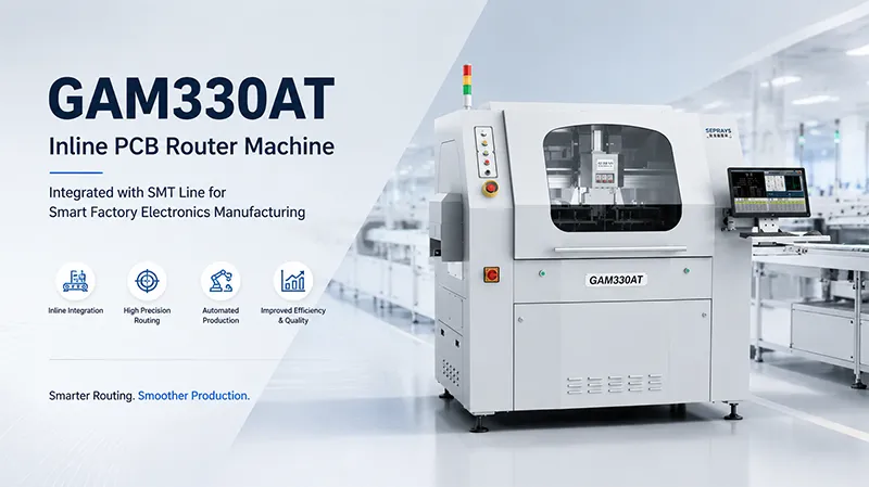
GAM330AT Inline PCB Router Machine Integrated with SMT Line for Smart Factory Electronics Manufacturing
PCB Router Machine integration has become an important topic for many electronics manufacturers as smart factories continue to develop. In the past, PCB depaneling was often treated as an independent finishing step after SMT assembly. A typical production flow looked like this: SMT placement → Reflow → Inspection → Manual transfer → PCB separation → Next process This approach can work well for small production volumes. However, as consumer electronics, industrial devices, communication products, and smart hardware continue to increase in complexity, many factories face a new challenge: The cutting process itself may not be the bottleneck. The real problem is the connection between processes. Manufacturers are now looking for solutions that can improve: The GAM330AT Inline PCB Router Machine is designed for this type of smart manufacturing environment, helping factories connect PCB separation with SMT production lines and reduce unnecessary manual handling. 🏭 Why Smart Factory Electronics Manufacturing Requires Better PCB Integration Modern electronics manufacturing is moving toward higher automation levels. Factories producing: often need to manage thousands of PCB assemblies every month. At this scale, traditional standalone equipment may create several challenges. Production Flow Becomes More Important A PCB separation process does not exist alone. It is connected