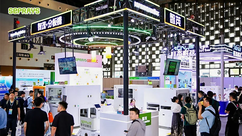
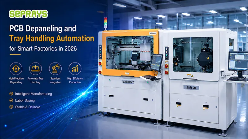
.png)

PCB Depaneling for High-Density PCBA has become a critical process as component spacing continues to shrink and functional integration increases. In modern SMT lines, routing is often the preferred depaneling method for dense layouts, but real-world production reveals recurring challenges that can affect yield, reliability, and long-term stability. This article summarizes practical lessons and proven fixes shared by engineers across global manufacturing sites.
⚙️ Why High-Density PCBA Is Especially Sensitive to Routing
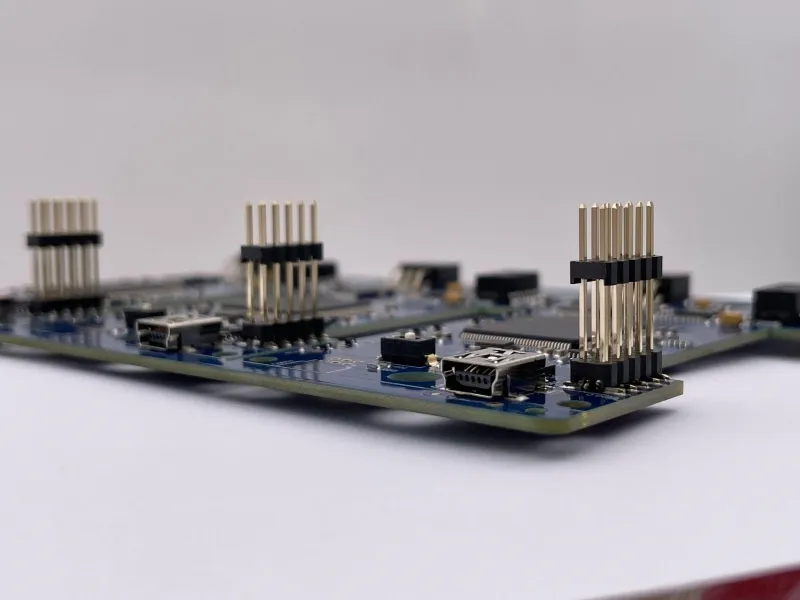
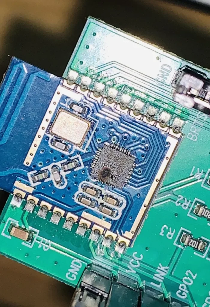
High-density PCBAs typically feature fine-pitch components, edge-mounted connectors, and multi-layer structures. During routing, even minor vibration or tool wear can transfer stress into solder joints or ceramic components.
Engineers frequently report:
- Micro-cracks forming near MLCCs close to board edges
- Burrs or fiber pull-out affecting insulation performance
- Panel flex during cutting causes latent defects
These issues often pass visual inspection but appear later during thermal cycling or vibration testing.
🧩 Challenge 1: Tool-Induced Vibration and Accuracy Drift
One of the most common routing challenges is vibration caused by spindle wear or improper parameter settings. Over long production runs, this can lead to inconsistent edge quality and increased mechanical stress.
Best fixes shared by production teams:
- Use high-rigidity spindles with controlled runout
- Match feed rate to PCB thickness and copper density
- Implement preventive tool replacement schedules
A high-density industrial control line reported a 20% yield improvement after tightening spindle maintenance intervals alone.

🪚 Challenge 2: Panel Support and Board Flex
Routing removes material gradually, but insufficient panel support can still allow flex—especially on thin or large-format panels.
Recommended practices include:
- Full-surface vacuum fixtures for thin boards
- Adaptive clamping for mixed panel designs
- Sequenced cutting paths to minimize stress buildup
Engineers note that better fixturing often delivers greater benefits than increasing machine accuracy.

🔧 Challenge 3: Dust, Debris, and Edge Contamination
Routing generates fine fiberglass and resin dust, which can settle near high-density components.
Field observations show that poor dust management leads to:
- Additional cleaning steps
- Increased inspection time
- Risk of conductive debris remaining on the board
Effective dust extraction close to the cutting point is increasingly viewed as a quality requirement rather than an optional feature.
📉 Cost Analysis: Routing Quality vs. Downstream Loss
For high-density PCBA, routing-related defects rarely stop the line immediately. Instead, they create downstream costs:
- Rework during functional testing
- Scrap discovered late in the process
- Customer returns are tied to intermittent failures
Several EMS providers report that investing in better routing control reduced total cost per board, even though equipment cost increased.
🏭 Case Insight: High-Density Communication Module
A communication equipment manufacturer experienced unexplained failures during vibration testing. Root-cause analysis traced the issue to routing-induced stress near edge connectors. After adjusting routing paths and improving panel support, failures were eliminated without changing PCB layout or components.
🛠️ Practical Takeaways for Engineers
Based on field experience, engineers recommend:
- Treat routing as a stress-sensitive process, not just a cutting step
- Monitor vibration and tool condition continuously
- Design fixtures specifically for high-density layouts
- Validate routing quality through reliability testing, not just AOI
These measures help align routing with industrial durability expectations.
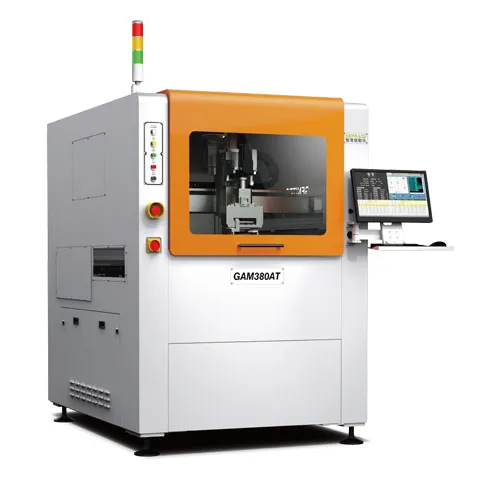
💬 Why Choose Seprays Group?
Seprays Group provides PCB depaneling solutions engineered for high-density applications, with a strong focus on industrial quality, durability, and process stability. We support manufacturers in optimizing routing performance under real production conditions rather than ideal test scenarios.
If you would like to discuss routing challenges in high-density PCBA or evaluate suitable depaneling solutions, please feel free to contact us.
WhatsApp: +8618929266433
E-mail: sales@seprays.com