.png)
Ultra-Precision PCB Depaneling is becoming a serious topic of discussion within semiconductor manufacturing facilities in 2026.
Not because it sounds advanced.
But because the margin for error is shrinking fast.
A semiconductor customer once shared something surprisingly simple during a factory visit:
“One tiny cutting deviation can ruin an entire high-value board.”
That statement stayed with many engineers in the room.
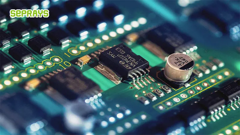
Today’s semiconductor PCBAs are:
- Smaller
- Denser
- More sensitive to mechanical stress
And the depaneling process — once considered a minor production step — is now directly tied to product reliability.
🔍 Why Semiconductor PCBAs Are More Difficult to Depanel Today
Five years ago, many depaneling systems could tolerate small process variations.
In 2026?
Not anymore.
Semiconductor-related PCBAs increasingly include:
- Fine-pitch components
- Thin substrates
- Dense BGA layouts
- High-layer-count boards
- Sensitive solder joints
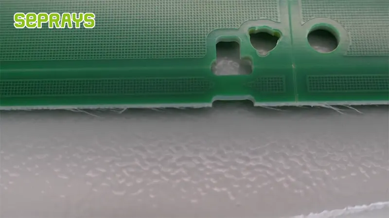
Some components are positioned extremely close to the board edge.
That changes everything.
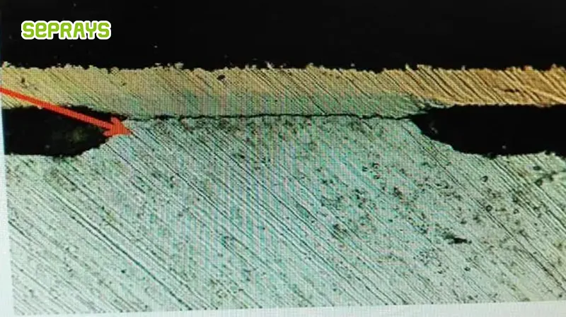
Even minor vibration or cutting stress may lead to:
- Invisible micro-cracks
- Solder fatigue
- Signal instability
- Long-term reliability risks
The difficult part?
Most defects are not immediately visible.
⚠️ The Hidden Cost of “Good Enough” Depaneling
One common misconception is:
“If the board looks fine after cutting, the process is acceptable.”
But semiconductor manufacturing rarely works that way.
A board can pass visual inspection while still containing:
- Internal stress damage
- Weak solder connections
- Microscopic fractures
These problems may only appear later during:
- Thermal cycling
- High-frequency operation
- Long-term field use
For semiconductor applications, delayed failure is often far more expensive than immediate scrap.
⚙️ Why Traditional Depaneling Methods Are Struggling
Older depaneling approaches still work for some standard PCB products.
But semiconductor PCBAs introduce new challenges.
Common issues include:
- Excessive mechanical stress
- Positioning deviation
- Edge burrs
- Dust contamination
- Inconsistent cutting quality
Especially in high-volume production, small instability becomes cumulative.
That means:
A tiny process deviation repeated thousands of times becomes a major yield problem.
🧩 What Semiconductor Manufacturers Actually Need
The conversation is no longer only about cutting speed.
Semiconductor manufacturers now prioritize:
- Micron-level accuracy
- Low-stress processing
- Stable repeatability
- Vision-guided alignment
- Automation compatibility
In many factories, yield stability matters more than raw machine speed.
That may sound counterintuitive.
But consistent precision usually saves more money than faster cutting alone.
📊 Traditional vs Ultra-Precision PCB Depaneling
| Factor | Traditional Depaneling | Ultra-Precision Depaneling |
|---|---|---|
| Position Accuracy | Moderate | Micron-level |
| Mechanical Stress | Higher | Very low |
| Suitability for Dense PCBAs | Limited | Excellent |
| Edge Quality | Variable | Stable |
| Automation Compatibility | Basic | Advanced |
| Semiconductor Reliability | Risky | Safer |
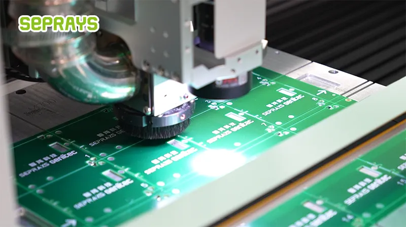
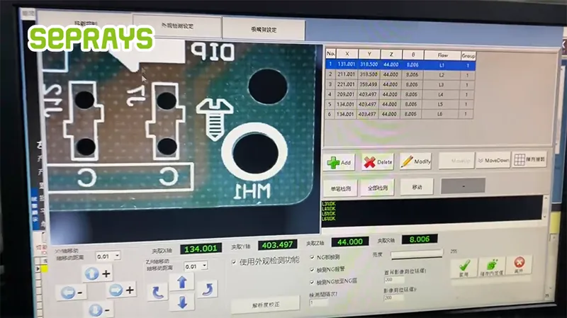
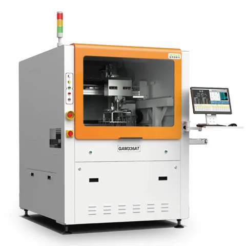
💡 Why CCD Vision Systems Matter More Than Ever
Modern semiconductor PCBAs leave little room for alignment error.
That is why CCD vision systems are becoming standard in advanced depaneling.
These systems automatically:
- Identify fiducial marks
- Correct board deviation
- Adjust cutting paths in real time
This becomes critical when:
- Panels shift slightly
- PCB dimensions vary
- Complex board shapes are involved
Without vision correction, even a small positioning drift can affect cutting quality.
🏭 Real Factory Challenge — High-Density Semiconductor PCBAs
A semiconductor electronics supplier faced recurring yield instability during depaneling.
Their boards featured:
- Tight component spacing
- Thin substrates
- Complex multi-board panels
The original process used traditional mechanical depaneling with manual alignment.
Problems included:
- Occasional edge damage
- Inconsistent positioning
- High operator dependency
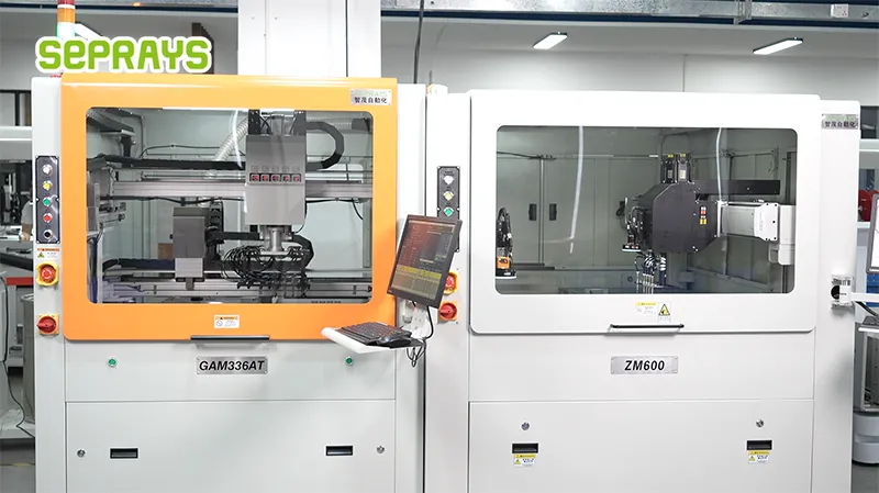
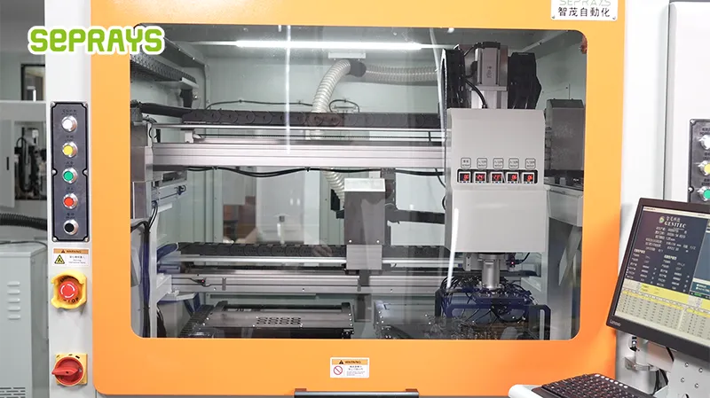
After evaluating process data, the factory worked with Seprays to upgrade the production line.
The new solution included:
- CCD vision alignment
- Low-stress routing technology
- Vacuum stabilization
- Automated handling support
The result was not just higher accuracy.
The more important improvement was the consistency of processes across batches.
That helped stabilize downstream inspection and assembly performance as well.
🔬 Why Semiconductor Boards Need Lower Stress Than Consumer Electronics
Not all PCBAs react to stress the same way.
Consumer products may tolerate small mechanical impact.
Semiconductor applications often cannot.
Especially in:
- AI servers
- Automotive chips
- Power modules
- High-frequency communication devices
- Industrial control systems
Low-stress depaneling becomes part of long-term reliability strategy.
Not just manufacturing efficiency.
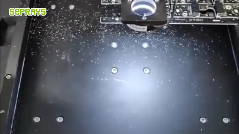
🚨 Another Overlooked Issue — Dust Contamination
Mechanical depaneling generates dust.
In semiconductor production, contamination control matters.
Poor dust extraction may affect:
- Sensitive components
- Inspection systems
- Machine stability
- Product cleanliness
That is why advanced depaneling systems increasingly integrate:
- High-efficiency dust collection
- Enclosed processing environments
- Automated cleaning systems
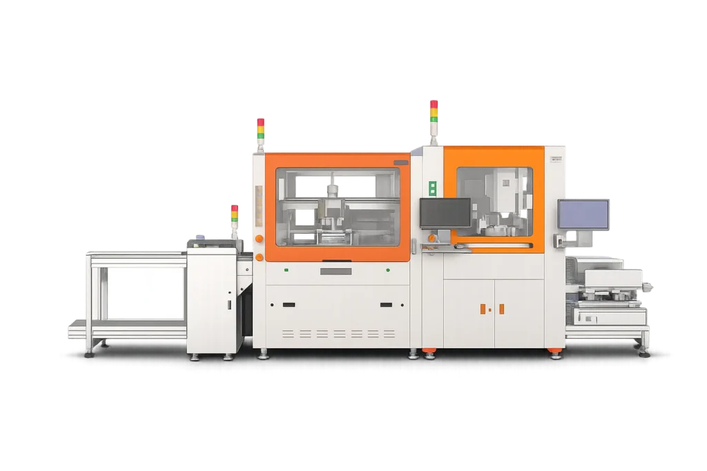
🔄 Why Automation Is Becoming Necessary
Labor variability creates risk in precision manufacturing.
In 2026, semiconductor factories are increasingly adopting:
- Inline depaneling
- Robotic loading/unloading
- Automated recipe switching
- Vision-guided processing
The goal is simple:
Reduce human variability while improving repeatability.
🌍 Industry Trend — Semiconductor Packaging Is Evolving Fast
Semiconductor packaging technology continues to evolve toward:
- Smaller form factors
- Higher integration
- More complex PCB structures
This trend directly affects depaneling requirements.
A process that worked three years ago may no longer meet reliability expectations today.
That is why many manufacturers are reassessing their depaneling process earlier than expected.
💰 Is Ultra-Precision Depaneling More Expensive?
Initially?
Yes.
But the long-term cost discussion is more complicated.
Factories also need to consider:
- Yield loss
- Rework cost
- Reliability failures
- Customer returns
- Downtime from unstable processes
In many semiconductor environments, preventing hidden defects delivers far greater savings over time.
🚀 Final Thoughts
Ultra-precision PCB depaneling is no longer a niche requirement.
For semiconductor manufacturers in 2026, it is increasingly becoming part of the reliability foundation.
As PCBAs become denser and more sensitive, traditional depaneling approaches face growing limitations.
Precision alone is not enough anymore.
Manufacturers also need:
- Stability
- Repeatability
- Low-stress processing
- Smart automation integration
Because in semiconductor manufacturing, even microscopic process variation can create significant downstream consequences.
🚀 Why Choose Seprays Group?
With more than 30 years of experience in PCB/FPC depaneling technology, Seprays Group helps manufacturers solve increasingly complex depaneling challenges in semiconductor, automotive, industrial, and high-reliability electronics production.
Seprays Group provides a full range of depaneling solutions—including milling-cutter depanelers, laser depanelers, V-groove depanelers, punching depanelers, and automated handling systems. Our equipment is trusted by globally recognized manufacturers such as Foxconn, Flextronics, State Grid, Luxshare, Compal, Wistron, China Electronics, Quanta, CRRC, China Aerospace, OPPO, ZTE, and Bosch. Seprays systems are widely used across factories in China and worldwide.
By combining CCD vision alignment, low-stress processing technology, automation integration, and real manufacturing experience, Seprays supports customers in improving yield stability, cutting precision, and long-term product reliability.
If you are evaluating ultra-precision PCB depaneling solutions for semiconductor manufacturing, feel free to contact us. Our team is ready to help assess the best solution for your production process.
WhatsApp: +8618929266433
E-mail: sales@seprays.com
❓ FAQ
1. Why is ultra-precision PCB depaneling important for semiconductor manufacturing?
Semiconductor PCBAs are highly sensitive to mechanical stress and positioning deviation.
2. What problems can poor depaneling cause?
Potential issues include micro-cracks, solder fatigue, edge damage, and long-term reliability failures.
3. Why are CCD vision systems important in semiconductor depaneling?
They improve alignment accuracy and reduce cutting deviation during high-precision processing.
4. Is laser depaneling always better for semiconductor PCBAs?
Not always. The best method depends on board structure, material, component layout, and production volume.
5. How does automation improve depaneling consistency?
Automation reduces operator variability and improves repeatability across large production batches.