.png)
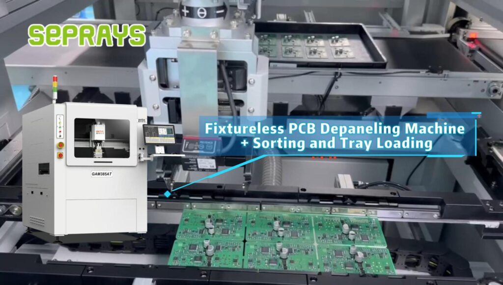
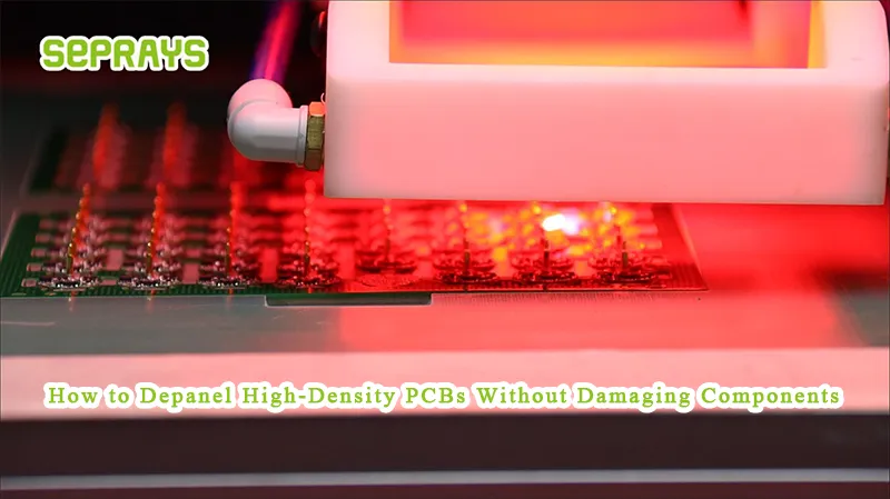
Fixtureless PCB Depaneling Machine solutions have become essential in modern SMT lines where board materials, component density, and outline geometry are more challenging than ever. Many production teams in Europe and North America continue to share similar questions: How do you keep panel stability under control? How do you avoid micro-cracks, edge stress, and material distortion when the PCB structure itself is fragile?
Below are field-tested insights gathered from different factories running daily high-precision operations.
🔧 H1 — The Real Pain Points Behind Warping and Thin PCB Panels
Warping is not only a material issue; it often increases when the panel size becomes larger or when the copper distribution is uneven. In Germany and France, engineers frequently point out three recurring problems:
- Residual mechanical stress inside laminate layers
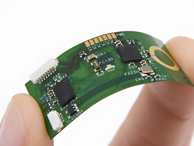
- Ultra-thin substrates (0.3–0.6 mm) bending during routing
- Non-symmetrical component placement, causing uneven heat absorption
In a fixture-based system, these variations often require dedicated jigs. With thin or flexible panels, jig tolerances can’t fully suppress deformation, leading to inconsistent cut depth and uneven tool pressure.
A fixture-free approach reduces constraint points and lets the machine adapt dynamically to the PCB’s natural condition instead of forcing it into a rigid shape.
⚙️ H2 — Cost Analysis: Where Manufacturers Lose Money Without Noticing
Across multiple SMT sites, costs typically accumulate in four quiet but critical places:
- High scrap rate due to micro-cracks in brittle substrates
- Additional fixture creation for every product variant
- Extended line downtime when switching models
- Tool wear from compensating for uneven panel deformation
For thin PCBs or irregular shapes, fixture design may become more expensive than the panel itself. Some French OEMs report fixture budgets exceeding thousands of euros per product family — a recurring cost that grows with every product revision.
A fixtureless depaneling process helps eliminate this hidden expense.
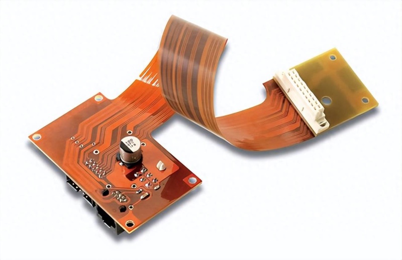
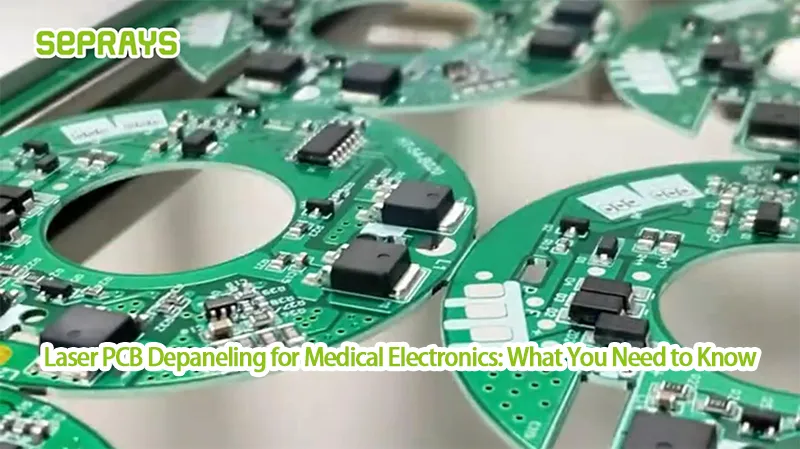
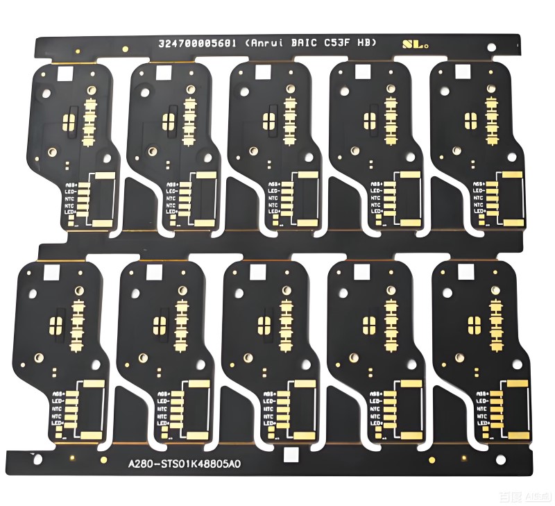
🧠 H3 — Case Observation: Complex Board Shapes in Automotive Electronics
A German automotive lighting manufacturer shared a typical scenario:
- PCB outline includes curved edges, internal slotsy asymmetric geometry
- Board thickness: 0.8 mm
- Surface components: high-profile and sensitive
- Annual volume: 1.5 million units
Traditional routing caused vibration marks and unpredictable board movement. Fixtureless routing with CCD correction stabilized the process by automatically recognizing the true panel position before every cut.
The scrap rate dropped from 2.1% to 0.3%, mainly because cutting deviation was reduced and clamp-free handling avoided stress concentration around the edges.
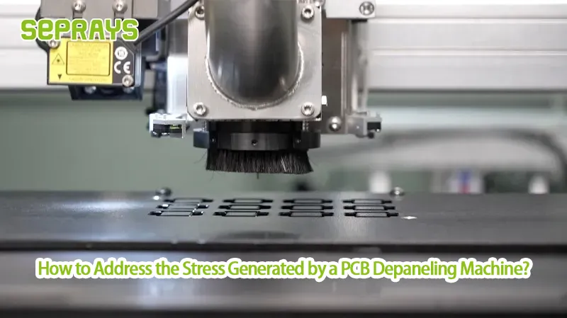
🛠️ H4 — Practical Solutions for Warping, Thin Materials, and Shape Variations
Here are process-driven solutions derived from real production teams:
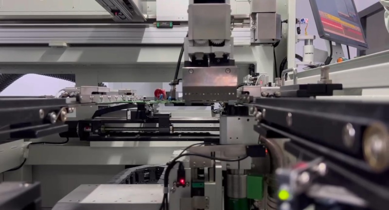
1. Adaptive vision correction
CCD recognition compensates for panel warp, rotation, and dimensional tolerance, improving consistent accuracy even on unstable materials.
2. Bottom-side cutting strategy
Cutting from the bottom minimizes component disturbance and distributes mechanical load more evenly, reducing stress on fragile parts.
3. Soft clamping & distributed support
Instead of a rigid fixture, soft pressure points support the PCB naturally, preventing bending forces from accumulating.
4. High-speed spindles with controlled load
A stable spindle (50,000–100,000 RPM) keeps tool force low, reducing burrs and minimizing edge chipping.
5. Route sequencing optimization
Cutting outer profiles last helps maintain structural integrity throughout the process.
These methods apply broadly across Europe, where production standards emphasize industrial durability, precision, and long-term reliability.
🧩 H5 — Discussion: When Does Fixtureless Depaneling Make the Most Sense?
From shared user experiences, fixture-free depaneling is particularly advantageous when:
- PCB thickness < 0.8 mm
- Component height prevents traditional clamping
- Frequent product changeovers increase fixture cost
- Board outlines require flexible routing strategies
- Warped panels reduce the success rate of fixed tooling
If these situations occur repeatedly in your factory, a fixtureless system can reduce long-term operational pressure.
⭐ Why Choose Seprays Group?
Seprays Group focuses on stable, industrial-grade PCB depaneling technology designed for factories seeking long-term durability, precise routing quality, and a fixture-free workflow. Our solutions are built around real manufacturing challenges — thin boards, flexible materials, and complex geometries — helping engineering teams maintain consistency and reduce hidden production costs.
If you need professional suggestions or want to discuss your current depaneling challenges, please contact us anytime.
WhatsApp: +8618929266433
E-mail: sales@seprays.com