.png)
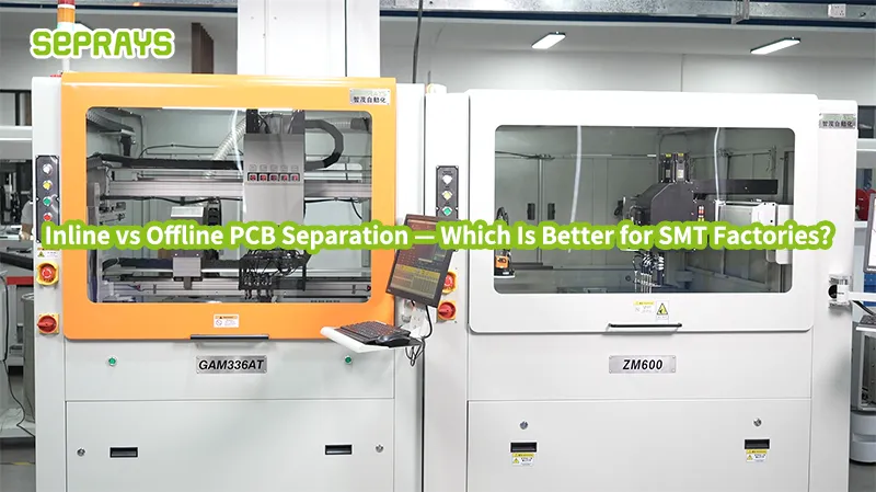
Inline vs Offline PCB Separation — Which Is Better for SMT Factories?
Inline PCB separation is becoming a hot topic among SMT manufacturers in 2026. Not because offline depaneling has disappeared. In fact, many successful factories still rely on offline systems every day. The real question is different: Which solution creates the best balance between productivity, flexibility, quality, and long-term operating costs? The answer depends on your production environment. A factory producing millions of identical automotive PCBs may need a completely different approach from an EMS provider handling dozens of product changes every week. This article explores the practical differences between inline and offline PCB separation from an engineer’s perspective. 🏭 Why More SMT Factories Are Re-Evaluating Their Depaneling Process Over the past few years, electronics manufacturing has changed significantly. Factories are facing: At the same time, PCB assemblies are becoming more complex. More components. Smaller spacing. Higher board values. As a result, depaneling is no longer viewed as a simple cutting process. It has become a critical part of overall manufacturing efficiency. ⚙️ What Is Inline PCB Separation? Inline PCB separation refers to depaneling equipment directly connected to the SMT production line. Boards move automatically from upstream processes into the depaneling system without manual intervention. The separated PCBs then continue to
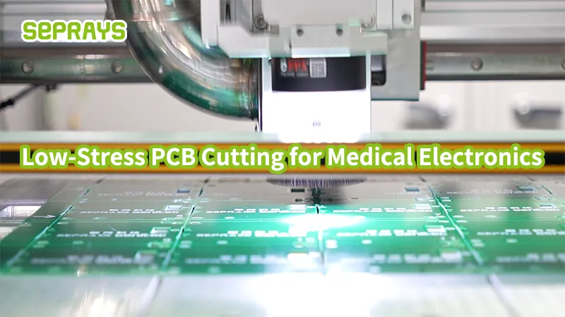
Low-Stress PCB Cutting for Medical Electronics
Low-stress PCB cutting is no longer optional in modern medical electronics production. Devices such as wearable monitors, implantable sensors, diagnostic instruments, and portable imaging systems demand not only precision but also extreme care during PCB separation. Even a small crack, micro-fracture, or stress-induced defect can compromise device reliability, regulatory compliance, and patient safety. In 2026, medical electronics manufacturers are focusing on cutting techniques that preserve PCB integrity while supporting high-throughput production. 🩺 Why Low-Stress PCB Cutting Matters in Medical Devices Medical electronics PCBs often have: High mechanical stress during depaneling can lead to: Factories that underestimate stress management risk: A low-stress cutting approach safeguards both quality and regulatory adherence. ⚙️ Common PCB Stress Points in Medical Production Even minor errors in depaneling can have outsized consequences. Stress Factor Production Impact Blade vibration Micro-cracks in FR4 or polyimide Excessive cutting force Component lifting or warping Poor alignment Misaligned traces, defective connections Manual handling Surface scratches, accidental flex High throughput without compensation Thermal stress, cumulative fatigue Interestingly, stress-induced failures are often invisible during visual inspection but become evident during reliability testing or after long-term use. 🔬 Seprays Case Study: High-Density Sensor Boards A leading medical electronics supplier producing multi-layer sensor boards struggled
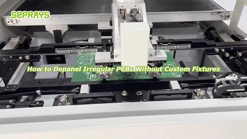
How to Depanel Irregular PCBs Without Custom Fixtures
Irregular PCB depaneling has become a growing challenge for electronics manufacturers in 2026. As PCB designs become smaller, more complex, and increasingly customized, many production teams are finding that traditional fixture-based depaneling methods no longer provide the flexibility they need. Circular boards. L-shaped boards. Sensor modules. Automotive control units. Wearable electronics. These products often feature unique outlines that make conventional fixtures expensive, time-consuming, and difficult to manage. The question many engineers are asking today is simple: Can irregular PCBs be depaneled accurately without custom fixtures? In many cases, the answer is yes. Modern vision-guided PCB router systems are making fixture-less production practical for a wide range of applications. 🔍Why Irregular PCB Shapes Create Manufacturing Challenges Not every PCB is designed as a simple rectangle. Today’s products often require: While these designs improve product performance, they create challenges during separation. Common production issues include: For high-mix manufacturing environments, these problems quickly become expensive. ⚠️The Hidden Cost of Custom Fixtures Many factories automatically assume that custom fixtures are necessary. However, the real cost is often underestimated. A fixture may seem inexpensive initially. But when production includes dozens of PCB models, costs accumulate rapidly. Typical Fixture-Related Expenses Cost Factor Impact Fixture design Engineering
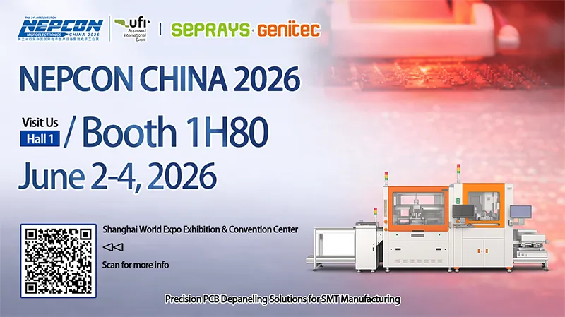
SEPRAYS & Genitec to Exhibit at NEPCON China 2026 – Hall 1, Booth 1H80
SEPRAYS and Genitec will join NEPCON China 2026.A key event for electronics manufacturing. The exhibition will be held from June 2 to 4, 2026.Venue: Shanghai World Expo Exhibition & Convention Center. Visit us at Hall 1, Booth 1H80. We will showcase precision PCB depaneling solutions.Focus on SMT manufacturing efficiency and stability. Our equipment supports high-precision PCB processing.Designed for modern automated production lines. Meet our team at the booth.Explore new technologies and application cases. Scan the QR code for more information.We look forward to seeing you in Shanghai. WhatsApp: +8618929266433 E-mail: sales@seprays.com
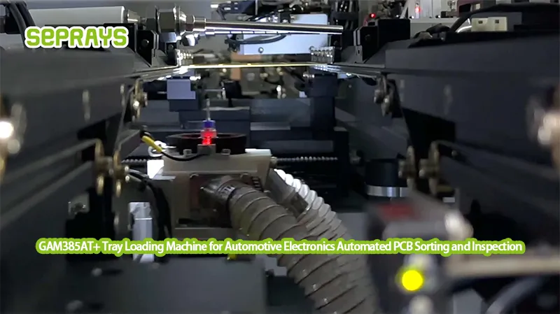
GAM385AT+ Tray Loading Machine for Automotive Electronics Automated PCB Sorting and Inspection
GAM385AT+ Tray Loading Machine solutions are becoming increasingly important in automotive electronics manufacturing.Not because factories simply want more automation.But modern PCB production lines can no longer afford unstable handling, manual sorting mistakes, or inconsistent inspection flow. In 2026, automotive electronics production is moving faster than ever. At the same time, manufacturers are facing: This is why automated PCB sorting and inspection systems are no longer optional for many SMT factories. They are becoming part of the core production strategy. 🚗 Why Automotive PCB Production Needs Automated Sorting Automotive electronics are different from standard consumer products. A small PCB defect can lead to: That changes how factories think about depaneling and inspection. In older production lines, operators manually handled: That process worked years ago. But today’s production volume and complexity expose its weaknesses. Especially during multi-shift production. ⚙️ What Problems Exist in Manual PCB Handling? Many SMT managers focus heavily on placement accuracy and AOI systems. But manual transfer between processes still creates hidden risks. Common Problems Seen in Factories Problem Production Impact Manual PCB sorting errors Wrong product mixing Inconsistent tray loading Transfer instability Delayed NG separation Rework confusion Operator fatigue Quality fluctuation Barcode mismatch Traceability issues Manual pallet handling
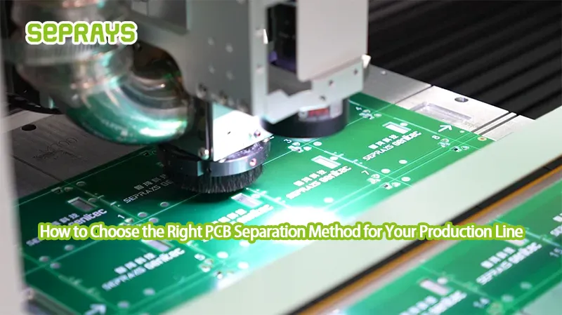
How to Choose the Right PCB Separation Method for Your Production Line
Selecting a PCB separation method has become a much bigger decision in 2026 than many factories expected.A few years ago, many manufacturers chose the lowest-cost depaneling machine available. Now the situation is different. Smaller components.Higher-density boards.Faster SMT lines.More EV and automotive projects.And tighter yield requirements. The wrong depaneling process can quietly increase: In many cases, the separation method affects SMT yield more than the cutting speed itself. So how do you actually choose the right PCB separation method for your production line? Let’s break it down from a real production perspective. 🔍 Why PCB Separation Is No Longer “Just a Cutting Step.” In older SMT factories, depaneling was often treated as a simple downstream operation. But modern electronics production changed the rules. Today’s PCBs often include: That means separation stress matters much more. One interesting trend in 2026:Factories are discovering that yield loss sometimes starts at depaneling — not SMT placement. Especially in: ⚙️ Common PCB Separation Methods in 2026 Different PCB structures require different cutting methods. There is no universal “best” option. Comparison Table Method Best For Advantages Limitations Router Depaneling Complex PCB outlines Flexible cutting paths, low stress Slower than saw cutting Saw Blade Depaneling Straight-line cutting High

