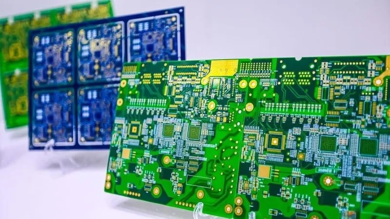
.png)
When should I choose router depaneling over V-cut?
The choice between router depaneling and V-cut largely depends on the design and requirements of your PCBA. While both are popular methods for separating boards, each method offers distinct advantages depending on factors like board thickness, component sensitivity, and precision needs. This article will explore when router depaneling is the better choice over V-cut, with a focus on practical considerations and real-world examples. ⚙️ What are the differences between router depaneling and V-cut? Before we discuss when router depaneling is preferred, let’s compare both methods briefly. V-Cut Depaneling: Router Depaneling: 🔍 When should you choose router depaneling over V-cut? Router depaneling is the preferred choice in the following situations: 1. Thicker PCBs or Rigid-Flex Designs For thicker boards (greater than 1mm) or rigid-flex PCBs, router depaneling provides the cutting power needed to maintain clean, stress-free separation. V-cuts are usually too shallow for thicker boards and may lead to breakage or incomplete separation, especially when dealing with multiple layers. Example:A medical device manufacturer needed to process rigid-flex boards with multiple layers of sensitive components. Router depaneling provided precise cuts without damaging internal layers or causing delamination. V-cut wasn’t an option because it didn’t offer enough depth to handle these complex materials.
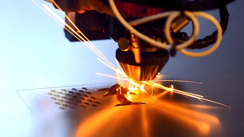
When should you choose laser depaneling over routing?
This is a common question for PCB and PCBA engineers facing tighter tolerances, denser layouts, and rising cost pressure. The short answer: choose laser depaneling when mechanical stress, edge quality, or design freedom becomes a limiting factor. Below is a practical, experience-based breakdown to help you decide. 🔍 Understanding the Core Difference Routing (milling) relies on physical contact between a rotating tool and the PCB. Laser depaneling, by contrast, uses a focused laser beam to separate boards without contact.The real difference shows up in stress, precision, and design flexibility—not just cutting speed. ⚠️ Key Pain Points with Traditional Routing Engineers often start questioning routing when they encounter these issues: Routing works well for many standard FR-4 panels, but as boards get thinner and layouts denser, its limits become visible. 🎯 When Laser Depaneling Makes More Sense You should seriously consider laser depaneling over routing if your project involves: In these scenarios, even well-optimized routing can introduce risks that are hard to eliminate. 💰 Cost Analysis – Looking Beyond the Machine At first glance, laser systems appear more expensive. But the total cost of ownership tells a different story: For low- to mid-volume, high-mix production, laser depaneling often balances out—or even
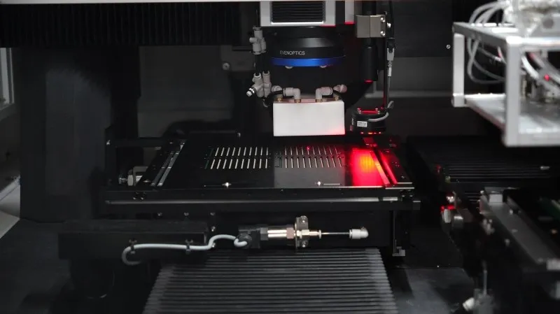
Is laser depaneling suitable for flexible PCBs?
Laser depaneling for flexible PCBs is increasingly popular in high-density electronics. Flexible PCBs are thin, stress-sensitive, and often densely populated. Mechanical methods like routing or V-cut can introduce micro-cracks, fiber pull-out, or board warping. Laser depaneling removes these risks, making it highly suitable when applied correctly. This article shares practical insights, production challenges, and cost considerations, with examples from EMS and OEM lines, including selective use of Seprays-supported laser depaneling. 🔍 Why Flexible PCBs Need Special Care Flexible PCBs bend and twist easily. Even minor mechanical stress during depaneling can lead to: For high-value products—automotive sensors, wearables, medical electronics—avoiding stress is critical. Laser depaneling eliminates mechanical contact, directly addressing these pain points. ⚙️ How Laser Depaneling Works on Flexible PCBs Laser depaneling uses a focused light beam to ablate PCB material without physical contact. Key effects for flex PCBs: Compared with routing, laser depaneling spreads cutting energy over time rather than applying instantaneous stress. ✨ Advantages of Laser Depaneling for Flexible PCBs Field experience shows these benefits: Flexible PCBs benefit more than rigid boards, especially in dense layouts or when components are close to the edge. 💡 Production Insights and Pain Points In real EMS lines: Introducing Seprays-supported laser depaneling,
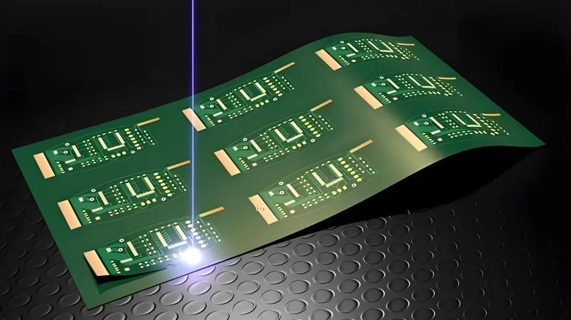
What PCB materials are suitable for laser depaneling?
PCB materials suitable for laser depaneling are not unlimited, and laser is not always the right answer. In real SMT production, laser depaneling performs extremely well for specific materials and use cases, while being less effective or inefficient for others. So instead of asking “Can laser cut this PCB?”, engineers usually ask a more practical question:“Is laser depaneling the most stable and cost-effective option for this material?” 🔍 The Short Answer First Laser depaneling is best suited for PCB materials that are: If your PCB falls into that category, a laser often solves problems that routing or V-cut cannot. ⚙️ PCB Materials That Work Well with Laser Depaneling From real production experience, these materials consistently perform well: 🟢 FPC and Rigid-Flex PCBs Laser depaneling is often the default choice here. 🟢 Thin FR4 (Standard & High-Tg) Most issues only appear when boards become thick or contain a lot of copper. 🟢 BT Resin and High-Precision Substrates These materials are often chosen because laser depaneling is available. ⚠️ Materials That Need Careful Evaluation Laser depaneling is not ideal for everything: Laser can still work—but only after trials and cost checks. In some cases, routing is simply more practical. 💡 Why Engineers
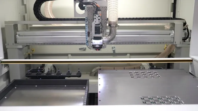
How close can components be to the PCB edge when milling depaneling?
Milling depaneling component-to-edge clearance is one of the most frequently debated topics between PCB designers, SMT engineers, and manufacturing teams. Everyone wants smaller boards, higher density, and lower cost—but routing physics does not disappear just because layouts become tighter. So, how close can components realistically be to the PCB edge when using milling depaneling? The answer is not a single number. It depends on how manufacturers define acceptable yield, as well as their process control standards and risk tolerance in real production. This article shares experience-based insights from global SMT lines, focusing on manufacturability, cost impact, and practical design–process coordination rather than theoretical limits. 🔍 Why Edge Clearance Becomes a Critical Question As PCBAs grow denser, edge space is often sacrificed first. However, insufficient clearance can lead to: Many issues are discovered too late—after tooling is already released. ⚙️ What Happens Physically During Milling Depaneling Milling depaneling removes material mechanically, which introduces: Even with a stable system, the PCB edge is not a “zero-stress zone.” Components placed too close together will feel that energy. 📏 Common Clearance Ranges Seen in Production Based on EMS and OEM field data, typical guidance looks like this: These are not hard rules—but probability curves.
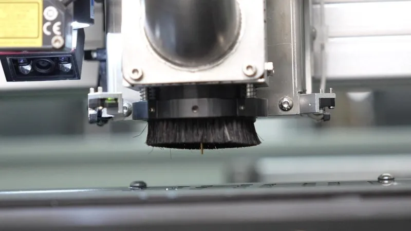
Will there be burrs after cutting the PCB with a milling cutter PCB depaneling machine?
Milling cutter PCB depaneling machine burr formation is one of the most common concerns raised by process engineers—especially when boards move directly into functional testing, coating, or final assembly. Burrs may look minor, but in high-density or high-reliability electronics, they can become a real quality risk. So, will burrs appear after milling and depaneling? The realistic answer is: they can—but they are controllable. This article shares production-level insights from EMS and OEM factories, focusing on industrial quality, durability, and practical process control rather than idealized claims. 🧠 What Engineers Mean by “Burrs” in PCB Depaneling In real production, burrs typically refer to: Not all burrs are equal. Some are cosmetic, while others can interfere with connectors, housings, or conformal coating. ⚙️ Why Burrs Occur During Milling Depaneling Milling is a mechanical cutting process, so burrs are influenced by multiple interacting factors: In many cases, burrs are not a machine problem—but a process setup issue. 🪚 Tooling Choices Make a Bigger Difference Than Expected Production data shows that the tooling strategy is often the deciding factor: Factories that shifted from time-based to cut-length-based tool replacement saw a clear reduction in burr-related rework. 🧩 Panel Support and Fixturing: An Overlooked Cause Insufficient

