.png)
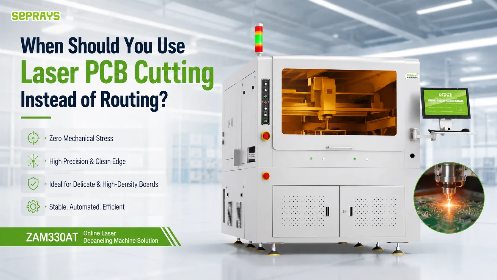
Laser depaneling instead of router depaneling is a question many engineers ask when PCB designs start getting smaller and more complex. In early production stages, router cutting may work well. But as component density increases and reliability requirements tighten, manufacturers often evaluate laser solutions.
This article shares practical insights from real production environments—looking at design limitations, cost considerations, and real-world manufacturing challenges.
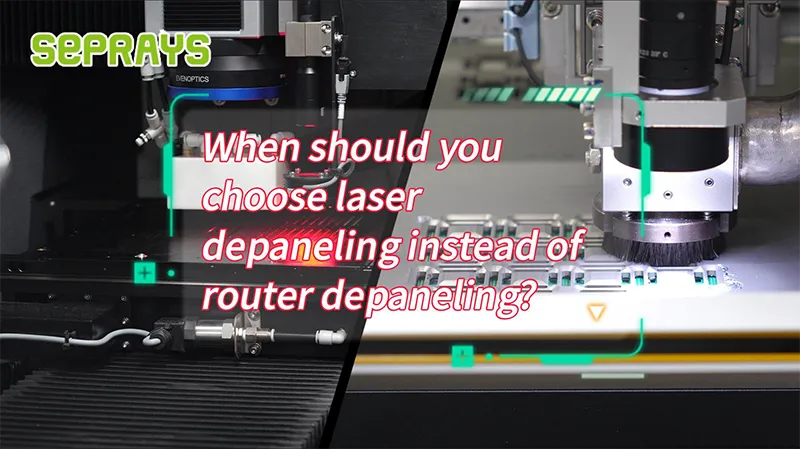
🔍 Understanding the Two Depaneling Methods
Before deciding which one to choose, it’s important to understand how the two processes differ.
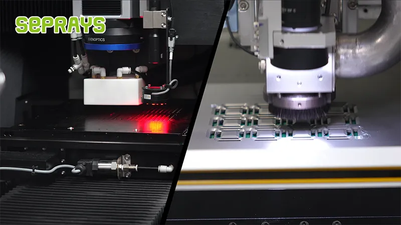
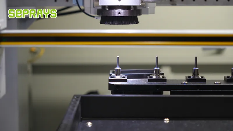
라우터 구분 separates PCBs using a high-speed rotating cutting bit. It physically mills the board along a programmed path.
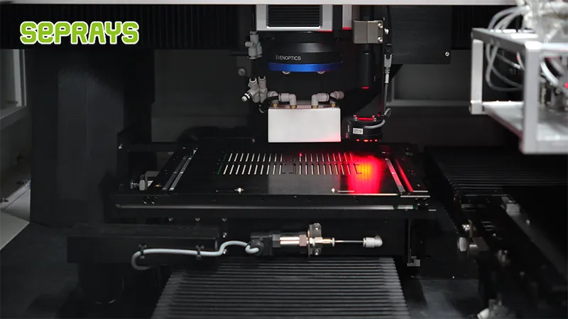
레이저 구분 uses a focused laser beam to cut the PCB without mechanical contact.
Both technologies are widely used across the electronics manufacturing industry. The difference lies mainly in mechanical stress, cutting precision, and flexibility for complex designs.
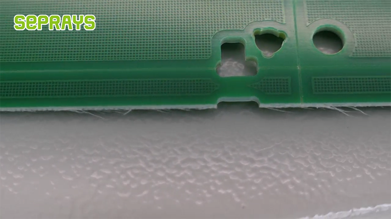
⚠️ The Hidden Problem — Mechanical Stress
One of the main reasons manufacturers move toward laser depaneling is the mechanical stress generated during router cutting.
When the router bit contacts the PCB, it produces vibration and cutting force. For traditional boards with enough edge clearance, this is usually acceptable. However, modern PCBs often place components extremely close to the board edge.
In these cases, router depaneling may cause:
- micro-cracks in solder joints
- damaged ceramic capacitors
- long-term reliability risks
- reduced manufacturing yield
These issues may not appear immediately during inspection, but they can affect product stability later in the field.
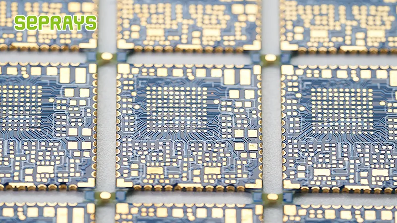
📏 PCB Designs Are Becoming More Compact
Today’s electronics products demand smaller and lighter devices. As a result, PCB layouts often leave very little space between components and board edges.
Typical examples include:
- wearable devices
- camera modules
- medical electronics
- RF communication modules
For these designs, minimizing stress during depaneling becomes critical. This is where laser depaneling, instead of router depaneling is often considered.
Laser systems cut the board without physical contact, greatly reducing mechanical influence on nearby components.
💰 Cost Considerations Beyond Machine Price
Many companies initially compare depaneling methods by looking only at machine cost. However, production reality involves more variables.
Some hidden costs include:
- component damage near board edges
- increased rework rates
- tool replacement and maintenance
- production downtime caused by tooling wear
Laser depaneling systems usually require a higher initial investment, but they eliminate cutting tool wear and reduce mechanical defects. For sensitive or high-value products, this difference can significantly impact overall manufacturing cost.
🧩 A Real Manufacturing Scenario
A consumer electronics manufacturer once faced recurring issues with compact communication modules. The PCB design placed components less than 0.6 mm from the edge, and router depaneling occasionally caused stress marks on solder joints.
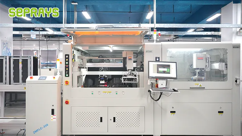
After evaluating alternatives, the engineering team introduced a laser depaneling solution from Seprays Group for this specific product line.
Over time, the production team observed:
- fewer edge-related defects
- improved yield stability
- more consistent cutting quality
The company still uses router depaneling for standard products, but relies on laser systems when board density and reliability requirements are higher.
🧠 When Engineers Typically Choose Laser Depaneling
In many factories, laser depaneling becomes the preferred solution under several conditions:
Laser depaneling is often selected when:
- components are located very close to the PCB edge
- boards are thin or fragile
- product reliability requirements are extremely high
- complex shapes require precise cutting paths
- flexible or rigid-flex PCBs are used
Meanwhile, router depaneling remains suitable for many traditional designs where cost efficiency and high throughput are the primary goals.
⚙️ Finding the Right Balance in Production
Instead of viewing laser and router depaneling as competitors, many manufacturers treat them as complementary technologies.
For example:
- router depaneling for standard rigid boards
- laser depaneling for delicate or high-density designs
This mixed approach allows production lines to maintain both efficiency and reliability depending on product requirements.
Ultimately, the decision should be based on PCB structure, component layout, and long-term product performance, not only equipment cost.
⭐ Why Choose Seprays Group?
Seprays Group focuses on advanced PCB depaneling technologies designed for modern electronics manufacturing. With experience supporting industries such as consumer electronics, automotive electronics, and medical devices, the company provides solutions including:
- laser PCB depaneling systems
- router depaneling machines
- precision depaneling automation solutions
By analyzing PCB structure, production scale, and reliability requirements, Seprays helps manufacturers choose the most suitable depaneling process for their applications.
If you are considering laser depaneling solutions for your production line, please feel free to contact us for more information.
WhatsApp: +8618929266433
이메일: sales@seprays.com