.png)

Best PCB Depaneling Machine: Common Mistakes Buyers Make During Selection
Best PCB Depaneling Machine selection is often treated as a purchasing task, but in reality, it is an engineering decision that affects product quality, yield stability, and long-term operating cost. Based on feedback from global SMT lines, many buyers encounter similar mistakes—not due to lack of effort, but due to incomplete evaluation criteria. ⚠️ Mistake 1: Focusing on Cutting Speed Instead of Board Stress One of the most common misconceptions is equating higher speed with higher productivity. While cycle time matters, engineers frequently report that excessive cutting force or vibration leads to hidden stress on components and solder joints. In high-density or thin PCB designs, stress-related microcracks may only appear after thermal cycling or field operation. The lesson shared by experienced SMT managers is clear: controlled force and stability often outweigh raw speed. 🧩 Mistake 2: Underestimating Long-Term Durability Initial performance during factory acceptance tests can be misleading. Buyers sometimes overlook spindle lifespan, mechanical rigidity, or dust management design. Over time, wear-related drift in accuracy leads to inconsistent results between shifts. From an industrial quality perspective, durability is not about how a machine performs on day one—but how predictably it performs after thousands of operating hours. 💰 Mistake 3: Incomplete
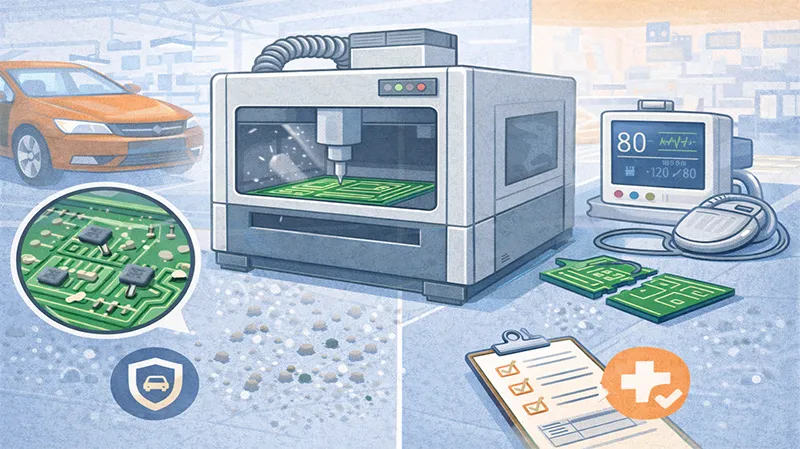
Dust-Free PCB Depaneling Machine: Lessons from Automotive and Medical PCB Assembly
Dust-free PCB Depaneling Machine solutions have become a critical topic in high-reliability electronics manufacturing, especially in automotive and medical PCB assembly. In recent years, global SMT lines have increasingly recognized that depaneling is no longer a “last step,” but a quality-defining process that directly affects reliability, compliance, and long-term product performance. ⚙️ Understanding Why Dust Control Matters in Critical Electronics In automotive and medical applications, even microscopic contamination can cause long-term risks. PCB dust generated during depaneling may appear harmless, but it can introduce conductive particles, weaken solder joints, or compromise insulation resistance. From discussions with Tier-1 automotive suppliers and medical OEMs, one common concern emerges: dust is difficult to detect immediately, yet its impact often appears months or years later in the field. This shifts the depaneling from a productivity topic to a lifecycle reliability issue. 🧪 User Pain Points Observed on Production Floors Manufacturing teams often raise similar challenges: In medical PCB assembly, compliance teams frequently require evidence that dust exposure is minimized and controlled. Traditional open depaneling methods make this difficult to document. 🧩 Cost Analysis: Prevention vs. Correction A dust-free depaneling approach does require higher upfront investment. Enclosed structures, vacuum extraction systems, and sealed cutting zones
PCB V-Cut Depaneling Machine: Practical Insights from High-Volume SMT Production
PCB V-Cut Depaneling Machine usage remains widespread in high-volume SMT production, particularly where board designs are standardized, and cost efficiency is critical. Despite the rise of routing and laser solutions, V-cut depaneling continues to play an important role in consumer electronics, power modules, and industrial products. This article shares practical insights from real SMT production lines rather than promotional comparisons. 🧱 Why V-Cut Still Matters in Mass Production In high-volume environments, simplicity and predictability are often valued over flexibility. Engineers working with V-cut depaneling emphasize that when PCB layout allows sufficient edge clearance, the process can be highly efficient. Key advantages frequently mentioned: For stable product designs with long production life cycles, these benefits remain attractive. ⚠️ Stress Behavior — The Primary Engineering Concern Mechanical stress is the most discussed limitation of V-cut depaneling. In practice, the separation force applied along the groove can affect solder joints and ceramic components. Common pain points reported: As component density increases, controlling break force becomes essential. Many SMT teams adjust scoring depth, blade angle, and separation speed to reduce stress concentration. ⚙️ Machine Durability in 24/7 Production In high-output factories, machines operate continuously. Engineers often evaluate V-cut equipment based on durability rather than

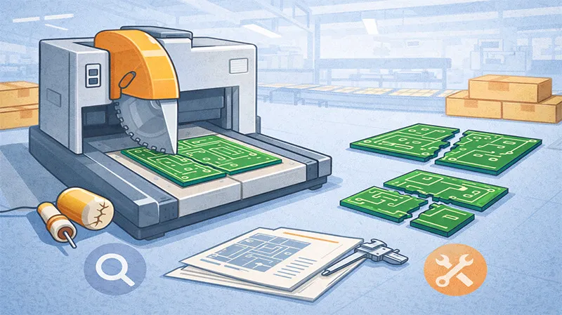
PCB Depaneling Machine Supplier: Router, Laser, or Blade Solutions Compared
PCB Depaneling Machine Supplier evaluation has become more complex as global SMT lines face increasing product diversity, thinner boards, and higher reliability expectations. Rather than asking which technology is “best,” engineers now compare router, laser, and blade solutions based on stress behavior, long-term stability, and total production cost. This article summarizes real-world insights shared across SMT production environments. ⚙️ Router Depaneling — Flexibility with Mechanical Control Router systems remain widely used due to their adaptability to complex PCB outlines and mixed production. Engineers commonly highlight: Pain points include vibration management, tool wear, and dust control. In long-term operation, machine rigidity and spindle stability largely determine whether routing remains consistent over months rather than weeks. 🔥 Laser Depaneling — Precision with Thermal Considerations Laser depaneling is increasingly applied in high-density and thin PCB applications where mechanical stress must be minimized. Key advantages discussed: However, engineers also point out limitations: As a result, laser solutions are often reserved for high-value electronics rather than general-purpose SMT lines. 🪚 Blade Depaneling — Strength for Rigid Applications Blade and saw-based systems are still relevant, particularly for thick or metal-core PCBs. Typical use cases include: While durable, blade systems introduce higher mechanical force and require careful
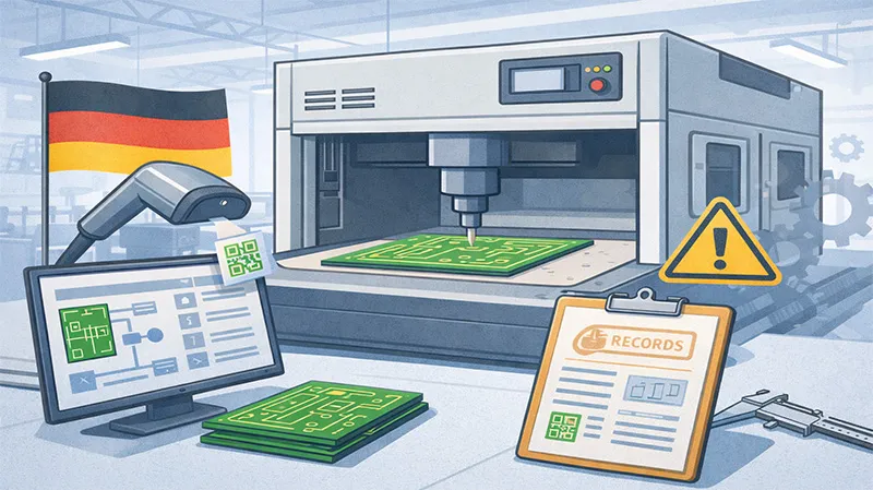
Inline PCB Router Depaneling System in Germany: Precision and Traceability Requirements
Inline PCB Router Depaneling System in Germany is often discussed among SMT engineers because German manufacturing places exceptional emphasis on precision, documentation, and long-term reliability. In automotive, industrial control, and high-reliability electronics, depaneling is no longer a simple separation step—it is a controlled process that must meet strict quality and traceability expectations. This article summarizes lessons shared by engineers working within German SMT environments. 🏭 Precision Expectations — Beyond Nominal Accuracy In German SMT lines, accuracy is evaluated over extended production periods rather than during initial acceptance tests. Engineers frequently point out that a system capable of ±0.05 mm accuracy on day one must maintain that level after months of continuous operation. Common challenges include: As a result, inline router systems are often assessed based on structural rigidity, thermal stability, and motion control consistency rather than advertised speed. 🔍 Traceability — A Non-Negotiable Requirement Traceability plays a central role in German electronics manufacturing. Depaneling systems are expected to integrate seamlessly with MES and line control systems. Key traceability requirements discussed by engineers: Without reliable traceability, downstream quality analysis and compliance reporting become difficult, increasing operational risk. ⚙️ Inline Integration — Stability Over Throughput Inline depaneling is valued for automation, but

Automatic PCB Router Machine vs V-Cut Systems: What Global SMT Lines Prefer
The comparison between Automatic PCB Router Machines and V-Cut Systems is a topic frequently discussed among global SMT engineers, especially as PCB designs become thinner, denser, and more reliability-driven. While both technologies remain widely used, real production experience shows that the choice is rarely about speed alone—it is about long-term process stability, stress control, and total cost of ownership. 🧱 Mechanical Impact — Stress Is the First Decision Point From an engineering perspective, the core difference lies in how each method applies force to the PCB. V-cut systems rely on mechanical separation along predefined grooves. While efficient, this approach introduces bending stress that can affect: Router-based systems remove material progressively, which significantly reduces mechanical stress. Many SMT lines report fewer latent defects when routing is used for high-density or sensitive assemblies. 🎯 Accuracy and Design Flexibility One recurring pain point shared by production teams is the frequency of design changes. V-cut advantages: However, limitations appear when: Automatic routing systems offer greater flexibility, supporting complex geometries and tighter tolerances, which align better with modern PCB layouts. ⚙️ Durability and Long-Term Stability In continuous SMT environments, equipment durability often matters more than peak throughput. Engineers frequently mention: Router machines, when built with

