.png)
PCB cutting without damage has become a bigger discussion point in electronics manufacturing in 2026. Many production teams are discovering that achieving a clean separation is no longer enough. The board may look perfect after depaneling, pass visual inspection, and even complete electrical testing successfully—but hidden stress can remain inside the assembly.
The problem is that damage is not always visible.
Tiny micro-cracks, weakened solder joints, edge chipping, and invisible stress around sensitive components may not appear immediately. In some cases, failures only emerge after vibration testing, thermal cycling, or long-term field use.
This creates an uncomfortable situation for manufacturers.
Everything appears normal at first.
Then, unexpected quality problems start showing up later.
For engineers working with increasingly compact products, avoiding damage during depaneling is becoming part of the entire reliability strategy rather than simply a cutting process.
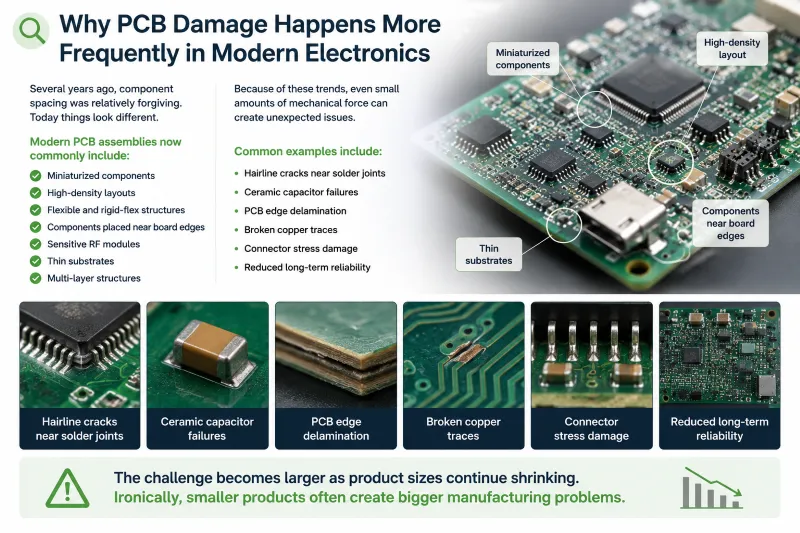
🔍 Why PCB Damage Happens More Frequently in Modern Electronics
Several years ago, component spacing was relatively forgiving.
Today, things look different.
Modern PCB assemblies now commonly include:
- Miniaturized components
- High-density layouts
- Flexible and rigid-flex structures
- Components placed near board edges
- Sensitive RF modules
- Thin substrates
- Multi-layer structures
Because of these trends, even small amounts of mechanical force can create unexpected issues.
Common examples include:
- Hairline cracks near solder joints
- Ceramic capacitor failures
- PCB edge delamination
- Broken copper traces
- Connector stress damage
- Reduced long-term reliability
The challenge becomes larger as product sizes continue shrinking.
Ironically, smaller products often create bigger manufacturing problems.
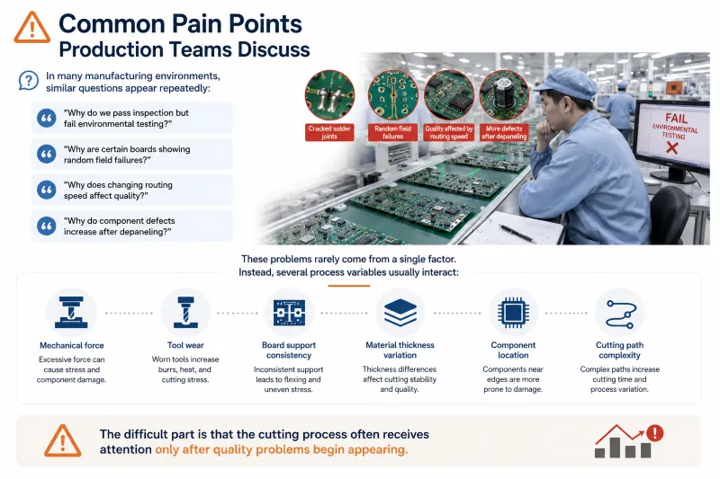
⚠️ Common Pain Points Production Teams Discuss
In many manufacturing environments, similar questions appear repeatedly:
“Why do we pass inspection but fail environmental testing?”
“Why are certain boards showing random field failures?”
“Why does changing routing speed affect quality?”
“Why do component defects increase after depaneling?”
These problems rarely come from a single factor.
Instead, several process variables usually interact:
- Mechanical force
- Tool wear
- Board support consistency
- Material thickness variation
- Component location
- Cutting path complexity
The difficult part is that the cutting process often receives attention only after quality problems begin appearing.
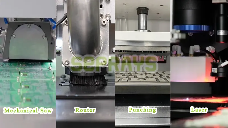
📊 Comparing Different PCB Separation Methods
Not every depaneling process creates the same stress profile.
| Method | Mechanical Stress | Edge Quality | Complex Shape Capability | Sensitive Component Compatibility |
|---|---|---|---|---|
| V-Groove Separation | Medium-High | Moderate | Limited | Moderate |
| Punching | High | Moderate | Low | Low |
| Router Depaneling | Low | Excellent | High | Good |
| Laser Depaneling | Extremely Low | Excellent | Excellent | Excellent |
Laser systems increasingly attract attention because they minimize physical contact during separation.
This matters particularly when component spacing becomes extremely tight.
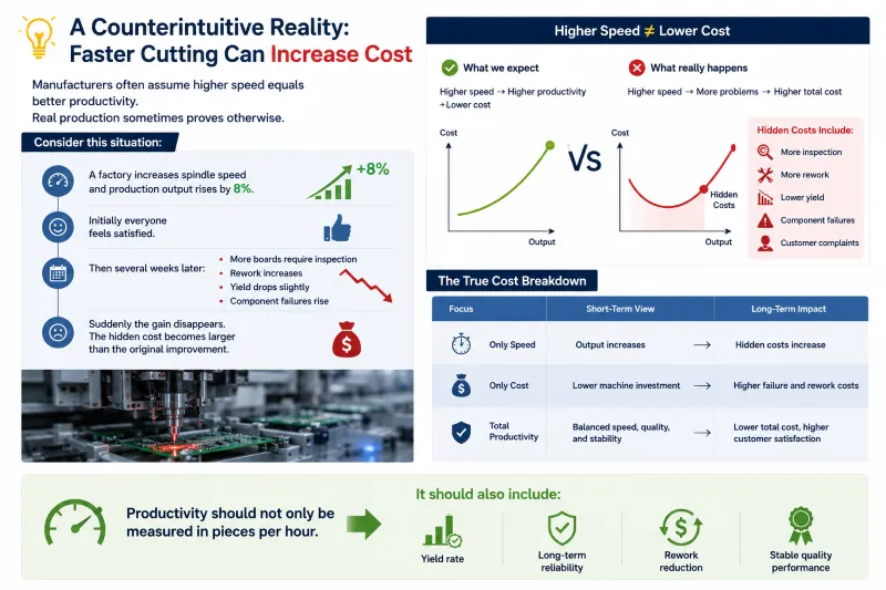
💡 A Counterintuitive Reality: Faster Cutting Can Increase Cost
Manufacturers often assume higher speed equals better productivity.
Real production sometimes proves otherwise.
Consider this situation:
A factory increases spindle speed, and production output rises by 8%.
Initially, everyone feels satisfied.
Then several weeks later:
- More boards require inspection
- Rework increases
- Yield drops slightly
- Component failures rise
Suddenly, the gain disappears.
The hidden cost becomes larger than the original improvement.
Productivity should not only be measured in pieces per hour.
It should also include:
- Yield rate
- Long-term reliability
- Rework reduction
- Stable quality performance
🏭 Real Manufacturing Example: Reducing Stress During Sensor Module Production
One electronics manufacturer producing communication modules experienced an unexpected issue.
The boards looked clean after separation.
Electrical testing also passed.
However, intermittent failures later appeared during vibration testing.
After the process investigation, engineers found several possible contributors:
- Components positioned near board edges
- Mechanical stress during separation
- Increasing board complexity
- Tight dimensional tolerances
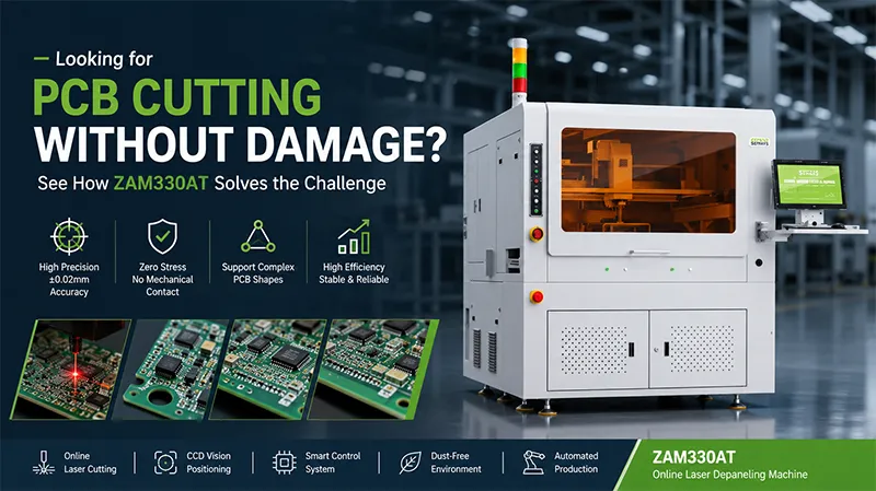
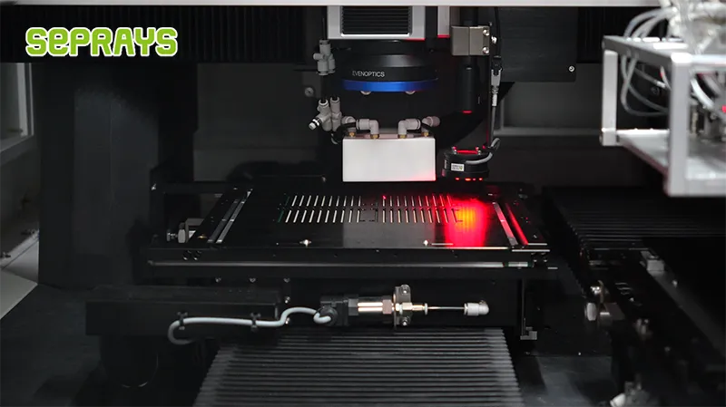
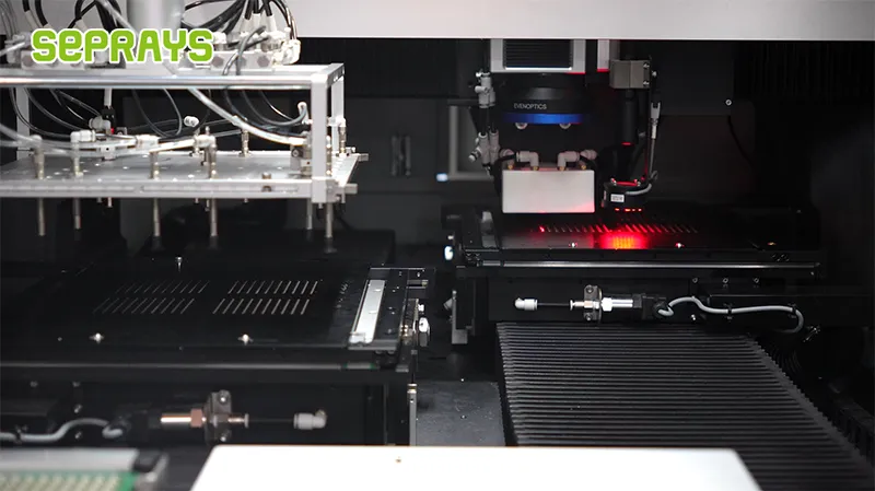
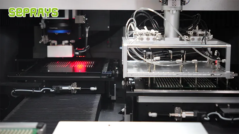
The production team later evaluated a laser depaneling process using a Seprays ZAM330AT Online Laser Depaneling Machine.
The goal was not simply to replace one machine.
The goal was to reduce invisible process risks.
Several observations followed:
- Reduced mechanical contact during separation
- Improved edge consistency
- Better handling of complex board geometries
- Lower process variation across production batches
Interestingly, the largest improvement was not in cutting speed.
It was confidence in long-term quality stability.
⚙️ How ZAM330AT Helps Address PCB Damage Challenges
The ZAM330AT Online Laser Depaneling Machine is designed for high-precision PCB separation environments where mechanical stress becomes a concern.
Several capabilities support this objective:
- Non-contact laser cutting process
- High positioning accuracy
- Support for complex PCB geometries
- Reduced stress during separation
- Inline automation capability
- Stable processing for sensitive assemblies
This becomes valuable when dealing with:
- Mobile electronics
- Communication products
- Automotive electronics
- Medical devices
- Sensor modules
- Thin PCB structures
🧠 Experience Correction: Zero Visible Damage Does Not Mean Zero Risk
This is an important lesson many engineers eventually learn.
A board can appear perfect visually while still containing hidden process stress.
Visual inspection only shows part of the picture.
Additional indicators matter:
- ✓ Reliability testing
- ✓ Thermal cycling performance
- ✓ Mechanical durability
- ✓ Long-term field behavior
Looking only at appearance sometimes creates misleading conclusions.
🔧 Questions Worth Asking Before Selecting a Depaneling Method
Before choosing equipment, many manufacturers evaluate:
- How close are components to the cutting path?
- Are board geometries becoming more complex?
- How sensitive are installed components?
- Will future designs become smaller?
- Is long-term reliability a major requirement?
The answers often reveal the most suitable direction for the process.
🎯 Final Thoughts
Electronics manufacturing in 2026 is becoming increasingly complex.
Smaller products and denser designs continue pushing traditional processes toward their limits.
PCB separation no longer serves only as a final cutting step.
It directly influences reliability, yield, and long-term product quality.
For many manufacturers, preventing damage early in production creates greater value than correcting failures later.
Why Choose Seprays Group?
For over 30 years, Seprays Group has continuously focused on PCB and FPC depaneling technologies while helping manufacturers improve production quality and automation capability.
Seprays Group has been dedicated to PCB/FPC depaneling technology, providing a full range of solutions—including milling-cutter, laser, V-groove, and punching depanelers, as well as automated handling systems.
Our equipment is trusted by leading manufacturers, including Foxconn, Flextronics, State Grid, Luxshare, Compal, Wistron, China Electronics, Quanta, CRRC, China Aerospace, OPPO, ZTE, and Bosch, with solutions operating across China and worldwide manufacturing facilities.
Why customers continue working with Seprays:
- 30+ years of industry experience
- Complete PCB/FPC depaneling solutions
- Support for smart factory automation
- Proven deployment across global production environments
- Technical customization capability
- Reliable after-sales service and long-term support
If you are evaluating solutions for PCB cutting without damage, please feel free to contact us.
WhatsApp: +8618929266433
E-mail: sales@seprays.com
FAQ
1. Why does PCB damage sometimes appear after testing rather than immediately?
Some stress-related issues remain invisible initially and only become noticeable during vibration, temperature cycling, or long-term operation.
2. Is laser depaneling always better than routing?
Not always. Laser systems perform especially well for highly sensitive boards, thin substrates, and complex geometries, while routing remains effective for many applications.
3. Can components close to PCB edges increase risk?
Yes. Components near cutting areas experience greater stress exposure and require more careful process control.
4. Is non-contact cutting safer for sensitive assemblies?
In many cases, yes, because reduced physical force can minimize stress-related risks.
5. Can ZAM330AT integrate with automated production lines?
Yes. ZAM330AT supports online processing and integration into automated manufacturing environments.