.png)
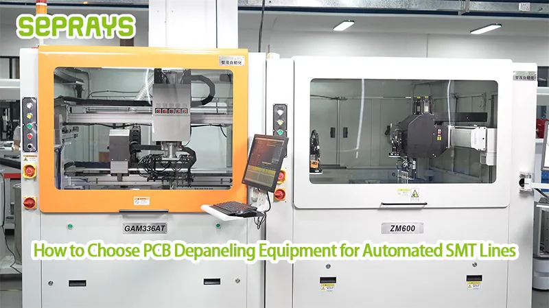
How to Choose PCB Depaneling Equipment for Automated SMT Lines
How to choose PCB depaneling equipment for automated SMT lines—this is usually not the first question engineers ask. It comes later, when the SMT line is already running fast, but something downstream can’t keep up. Boards pile up.Operators step in.Consistency drops. That’s when depaneling becomes a real decision point, not just a supporting process. ⚙️ Start from the SMT Line, Not the Machine A common mistake is choosing equipment based on specs alone. In automated SMT lines, what matters more is: Depaneling is not isolated.It must fit into the full production flow. Ask first: Without this, even the best machine won’t solve the problem. 🔍 Understand Your PCB Characteristics Different boards require different depaneling methods. Key factors include: For example: The board design defines the process. Not the other way around. 🧩 Matching Depaneling Methods to Applications Here’s a practical comparison for automated SMT environments: Method Stress Level Flexibility Automation Fit Typical Use Saw Blade Medium Low High Straight-line, high-volume boards Router Low-Medium High High Complex shapes, mixed production Laser Very Low Very High Medium-High High-density, sensitive PCBs V-Groove Low Medium High Pre-scored panels Punching Medium Low Very High Standardized mass production Each method can be automated.But not every method
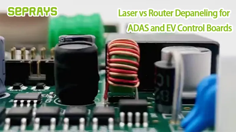
Laser vs Router Depaneling for ADAS and EV Control Boards
Laser vs router depaneling for ADAS and EV control boards is not just a technical comparison—it’s a decision that directly affects reliability, yield, and long-term performance. In automotive electronics, especially for ADAS modules and EV control units, even minor defects introduced during depaneling can lead to serious consequences down the line. So how do manufacturers choose between these two methods? 🚗 Why ADAS and EV Boards Demand More ADAS and EV control boards are different from standard PCBs. They often feature: This means the depaneling process must balance precision, stress control, and efficiency. Any compromise shows up later—in testing or in the field. ⚙️ Understanding Laser Depaneling Laser depaneling is a non-contact process. No physical force is applied to the PCB. Key characteristics: For ADAS sensors or camera modules, this level of precision is often critical. But there are trade-offs. 🔧 Understanding Router Depaneling Router depaneling uses a high-speed milling cutter. It physically removes material along the cutting path. Key advantages: It’s a mature and reliable solution. Especially when board designs are not extremely sensitive. 🔍 Direct Comparison — Laser vs Router Here’s a practical comparison based on real applications: Factor Laser Depaneling Router Depaneling Stress Level Very Low Low-Medium
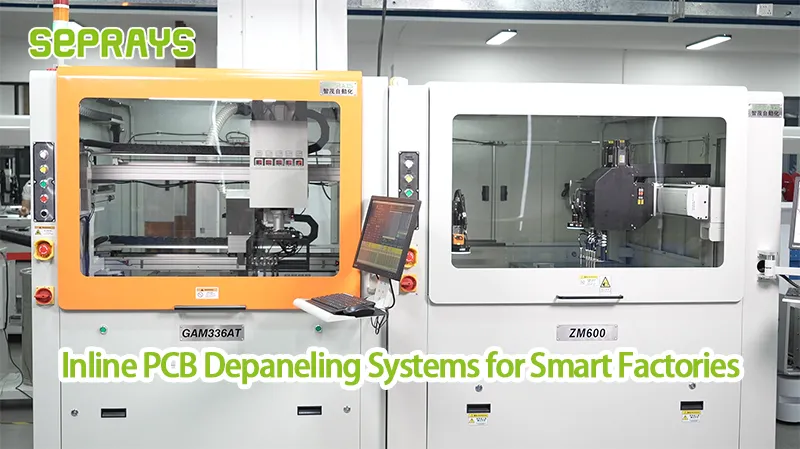
Inline PCB Depaneling Systems for Smart Factories
Inline PCB depaneling systems for smart factories are no longer just an upgrade option—they’re becoming a standard requirement. As production lines move toward full automation, the gap between SMT output and manual depaneling is increasingly difficult to ignore. Many factories don’t notice the problem at first.Until throughput drops.Or labor costs rise.Or quality becomes inconsistent. That’s where inline systems start to make sense. 🏭 Why Inline Depaneling Matters in Smart Manufacturing Smart factories are built on flow. Every process is connected.Every delay spreads downstream. Traditional offline depaneling creates friction: Inline PCB depaneling systems remove these gaps. Boards move directly from SMT to separation.No extra steps.No unnecessary pauses. ⚙️ Key Benefits of Inline PCB Depaneling Systems From real production environments, a few advantages stand out: In short, it aligns depaneling with the logic of smart factories. 🚧 H2: Common Pain Points Before Going Inline Before adopting inline systems, many manufacturers faced similar issues: These problems don’t always come from poor equipment. They come from disconnected processes. Inline depaneling addresses the root cause—lack of integration. 🔍 Types of Inline Depaneling Solutions Not all inline systems are the same. Choosing the right type depends on your PCB design and production goals. Method Stress Level
Best PCB Depaneling Machines for EV and Automotive Electronics Manufacturing
Best PCB depaneling machines for EV and automotive electronics manufacturing—this isn’t just about equipment choice. It’s about reliability under harsh conditions, long product lifecycles, and zero tolerance for failure. In automotive electronics, even a small defect introduced during depaneling can lead to serious downstream risks. So the question becomes practical: which machines actually meet these demands? 🚗 Why Automotive PCBs Are Different Automotive and EV applications are not typical consumer electronics. They involve: Depaneling here is not just separation. It’s a quality control point. Any stress, burr, or micro-crack can compromise long-term performance. ⚙️ Key Challenges in EV PCB Depaneling From real production environments, several issues appear repeatedly: These are not isolated problems. They directly impact yield, cost, and delivery timelines. 🔍 Comparing Depaneling Machine Options Different depaneling machines solve different problems. Here’s a practical comparison based on automotive use: Method Stress Level Precision Speed Suitable Applications Saw Blade Machine Medium Medium High Power boards, straight cuts Router Machine Low-Medium High Medium Complex shapes, mixed layouts Laser Machine Very Low Very High Medium Sensitive circuits, high-density PCBs Punching Machine Medium Medium Very High High-volume, simple boards V-Groove Machine Low Medium Medium Pre-scored automotive panels No single method fits all. In
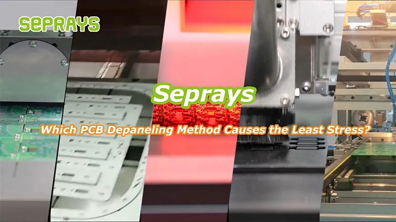
Seprays Group: Which PCB Depaneling Method Causes the Least Stress?
Which PCB depaneling method causes the least stress? For engineers and production managers, this question often arises when dealing with sensitive PCBs. In SMT manufacturing, edge cracks, micro-stress, and component damage can lead to rework, delays, and higher costs. Choosing the right depaneling technique is critical to maintain quality and throughput. 🔧 Understanding Stress in PCB Depaneling Stress in depaneling arises from mechanical force, vibration, or heat. Methods like sawing and punching physically push the board, which can: Reducing these stresses is essential for fragile, high-density, or multi-layer PCBs. ⚡ Comparing Common Depaneling Methods Not all methods affect boards the same way. Here’s a practical overview: Method Stress Level Best Use Case Speed Cost Notes Saw Blade Medium Straight-line V-groove boards High Low Fast but can cause mechanical stress on edges Router / Milling Low-Medium Complex shapes Medium Medium Cleaner edges, less vibration, suitable for irregular designs Laser Depaneling Very Low Sensitive, thin, high-density PCBs Medium High Non-contact, minimal stress, excellent for delicate components Punching / Stamping Medium High-volume standard boards Very High Low Quick but mechanical impact can stress solder joints V-Groove Breakout Low Straight-line boards Medium Low Controlled snapping, low mechanical stress if properly designed From this comparison,
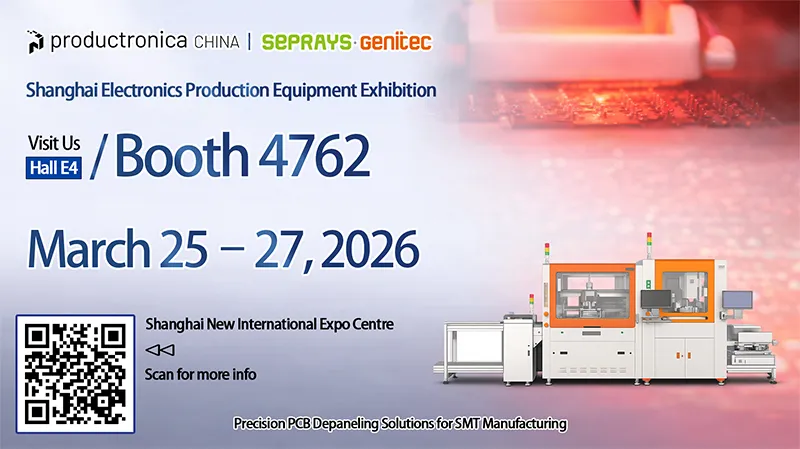
Join Us at Productronica China 2026
The global electronics manufacturing industry continues to evolve rapidly, driven by increasing demands for precision, efficiency, and automation. As one of the leading events in this field, productronica China brings together innovators, engineers, and manufacturers worldwide. In 2026, SEPRAYS and Genitec will be present at this important exhibition, showcasing advanced solutions designed to address real challenges in SMT production environments. 📍 Where to Find Us We invite you to visit us at: Whether you are exploring new technologies or looking to optimize your current production line, our team will be ready to discuss practical solutions tailored to your needs. ⚙️ What We’ll Be Showcasing At the booth, we will present our latest precision PCB depaneling solutions for SMT manufacturing. These systems are developed to meet the increasing complexity of modern electronic products. Key highlights include: 🚀 Why Precision Depaneling Matters In SMT manufacturing, depaneling is more than a finishing step—it directly affects product quality, yield, and operational efficiency. Poor depaneling processes can lead to: By adopting advanced depaneling technologies, manufacturers can reduce these risks while improving overall line performance. 🤝 Let’s Connect in Shanghai Industry challenges are constantly evolving, and finding the right solution often starts with the right conversation.

