.png)
 Russian
  English
  Spanish
  Japanese
  Korean
  Chinese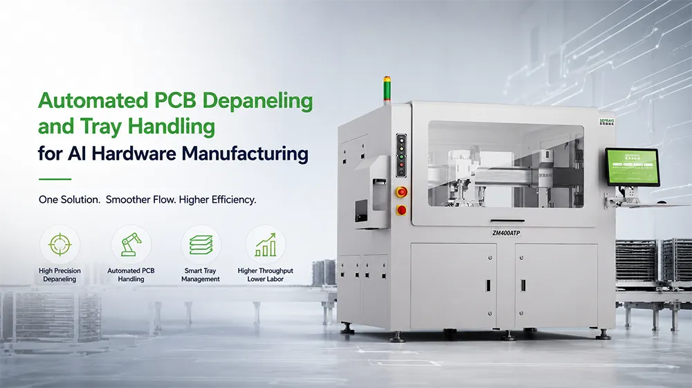
Automated PCB Depaneling and Tray Handling for AI Hardware Manufacturing
Automated PCB depaneling is becoming more relevant as AI hardware moves from engineering samples into higher-volume production. For a factory, however, the challenge is not simply separating PCBs faster. The bigger question is what happens after separation. Who removes the finished boards?Where are they placed?How are trays exchanged?How much operator handling is still required? When production runs across multiple shifts, these small steps can become a surprisingly large part of the manufacturing cost. 🤖 Why AI Hardware Needs a Different Production Approach AI servers, accelerator systems, communication equipment, and other high-performance electronics often use densely populated PCB assemblies. Manufacturers can separate and transfer multiple boards from a single panel without unnecessary handling. At low volume, operators can manage this process manually. At high volume, the situation changes. Repeated handling can introduce: The problem is not always the cutting operation itself. The real bottleneck may be material handling. 🔄 Depaneling Is Only One Part of the Cycle Consider a typical production sequence: Panel feeding → positioning → cutting → PCB transfer → tray loading → tray stacking A conventional machine may solve only the cutting step. The rest still depends on operators. That can make the overall line slower than expected.
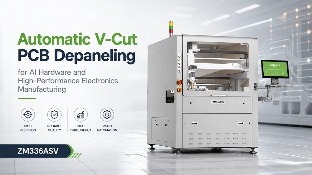
Automatic V-Cut PCB Depaneling for AI Hardware and High-Performance Electronics Manufacturing
Automatic V-Cut PCB depaneling becomes much more interesting when PCB production moves into AI servers, edge computing equipment, accelerator systems, and other high-performance electronics. The cutting operation itself is not complicated. The challenge is keeping the process consistent, clean, repeatable, and economical when production volumes increase. For manufacturers, the real question is not simply, “How fast can the boards be separated?” It is: Can the depaneling process keep up with production without creating quality or labor problems? 🤖 Why AI Hardware Changes the Production Equation AI hardware is putting more pressure on electronics manufacturers. High-performance computing systems can contain dense PCB assemblies, power-management boards, control boards, communication modules, and other electronic assemblies. These products often bring several manufacturing requirements together: A PCB may already have a V-groove design, making V-Cut separation a practical option. But when production reaches several shifts per day, manually separating those panels can become a bottleneck. That is where automation starts to make economic sense. 🔍 Start With the PCB Design Not every PCB should use V-Cut separation. Before choosing equipment, check: Panel sizeCan the machine accommodate the complete panel? PCB thicknessDifferent materials and thicknesses can behave differently during separation. V-groove designConfirm the groove position, depth,
How PCB Depaneling Supports the Growing Humanoid Robot Electronics Industry in 2026
PCB depaneling may not be the first thing people think about when discussing humanoid robots. Most attention goes to AI chips, actuators, batteries, sensors, and dexterous hands. But once a robot moves from a prototype to a production line, the electronics inside it become a manufacturing problem too. In August 2026, the second World Humanoid Robot Games in Beijing brought together 2,056 humanoid robots from 666 teams across 16 countries. More importantly, the event expanded beyond sports into factories, logistics, hotels, homes, and other real-world scenarios. That shift matters to electronics manufacturers. A robot that performs well in a demonstration still needs reliable, repeatable PCBA production before it can become a commercial product. 🤖 Why Humanoid Robots Create New PCB Challenges A humanoid robot is not built around one simple control board. Depending on the architecture, it may contain electronics for: These boards can have different sizes, shapes, component densities, and production volumes. A prototype may only require a few panels each week. A commercial product can require a completely different manufacturing strategy. This is where depaneling becomes part of the larger production discussion. 🔧 From Prototype Production to Mass Manufacturing The manufacturing process often changes as robot production scales.
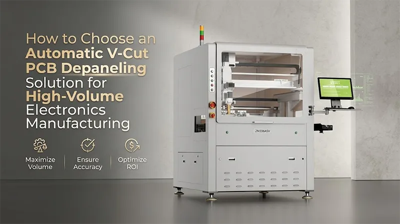
How to Choose an Automatic V-Cut PCB Depaneling Solution for High-Volume Electronics Manufacturing
Automatic V-Cut PCB depaneling solution selection often starts with one question: How fast can it separate our panels? In a real factory, that is only part of the answer. If production is running multiple shifts, operators are handling hundreds or thousands of panels, and product changeovers happen regularly, the bigger issue is consistency. A machine must fit the PCB design, production rhythm, quality requirements, and downstream process. The right choice is not necessarily the fastest machine. It is the one that removes the bottleneck without creating another one. 🔍 Start With the PCB, Not the Machine V-Cut separation works best when boards already have clearly defined V-grooves. Before comparing equipment, check: For example, a panel with straight V-grooves may be well suited to automated separation. A PCB with complex internal cutouts may be better handled by routing. This boundary condition matters. Automation cannot compensate for an unsuitable separation method. The ZM336ASV/ZM336ASVL, for example, is designed for V-Cut and V-Groove separation and supports X/Y-axis processing. Its valid cutting sizes are 330 × 280 mm and 430 × 400 mm, respectively. ⚙️ Look at the Complete Production Cycle Cutting speed is easy to compare. Total cycle time is harder. A high-volume process
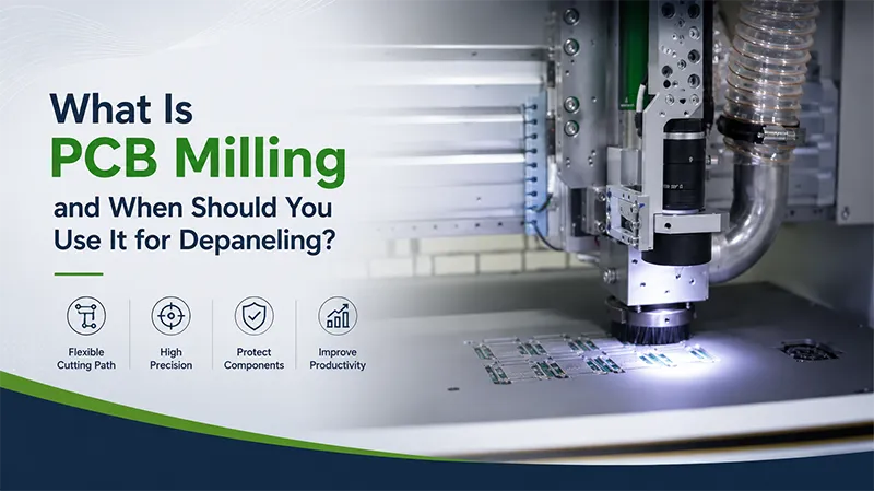
What Is PCB Milling and When Should You Use It for Depaneling?
PCB milling is one of those processes that look simple until the PCB becomes more complex. The basic idea is straightforward: a high-speed rotating cutter follows a programmed path and separates individual boards from a larger panel. But once components move close to the edge, board shapes become irregular, or production volumes increase, the choice of depaneling method becomes much more important. For many manufacturers, the real question is not simply “Can milling cut this PCB?” It is: “Will milling give us the right balance of accuracy, board protection, flexibility, and production cost?” 🔍 What Is PCB Milling? PCB milling uses a rotating cutting tool to remove material along a defined path. Unlike V-groove separation, it does not require the PCB to follow a straight pre-scored line. The cutting path can be programmed according to the board outline. That makes the process particularly useful for: Modern milling systems can also combine positioning, dust extraction, vision alignment, automatic tool changing, and material handling. Seprays, for example, offers both offline and in-line routing systems for different production requirements. ⚙️ How Does the Milling Process Work? A typical production cycle looks like this: Panel loading → PCB positioning → cutting-path recognition → milling
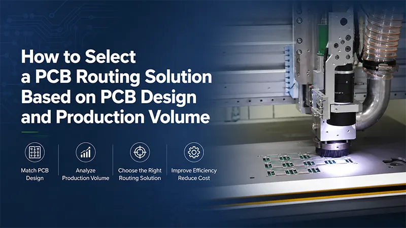
How to Select a PCB Routing Solution Based on PCB Design and Production Volume
PCB routing solution selection often starts with a machine quotation. That is understandable. Purchasing teams want to know the price, cutting speed, and delivery time. But engineers usually discover something else during production: the right machine depends much more on the PCB itself and how many boards the factory needs to process. A routing system that works well for a 500-panel monthly production may be completely different from one running several thousand panels per day. So, before comparing models, start with two questions: What does the PCB look like? And how much production does it need to handle? 🔍 Start With the PCB Design PCB geometry should be the first filter. If the panel has irregular outlines, internal cutouts, narrow tabs, or components positioned close to the edge, routing can offer more flexibility than simple V-groove separation. For straight, predictable V-grooves, however, a V-groove solution may be more economical. For very sensitive or high-value boards where mechanical stress is a major concern, laser processing may deserve evaluation. A practical first check includes: The important point is that not every PCB needs the same separation technology. Seprays’ current portfolio reflects this difference, covering routing, laser, V-groove, punching, and automated handling solutions.