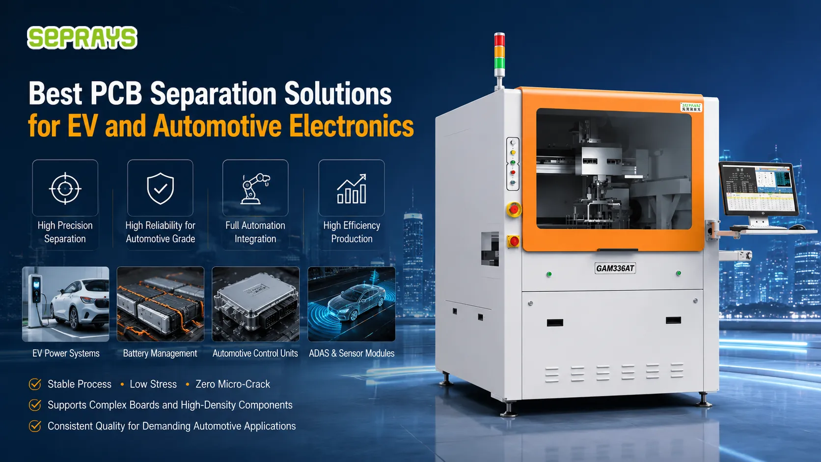
.png)
Mobile phone power adapter PCBs are getting smaller every year. Faster charging requirements, adoption of GaN technology, and more compact product designs are pushing components closer together than many manufacturers expected a few years ago.
On paper, the design looks efficient.
On the production floor, it often creates a different discussion.
Engineers start noticing small but frustrating problems:
Cracked solder joints.
Damaged edge components.
Micro-stress around sensitive ICs.
Unexpected yield drops.
And sometimes the depaneling process becomes the last place people investigate.
The issue is that power adapter boards are no longer simple rectangular PCBs with large empty margins. In many cases, components sit only a few millimeters—or even less—from the board edge.
A separation process that worked perfectly in 2022 may not be sufficient in 2026.
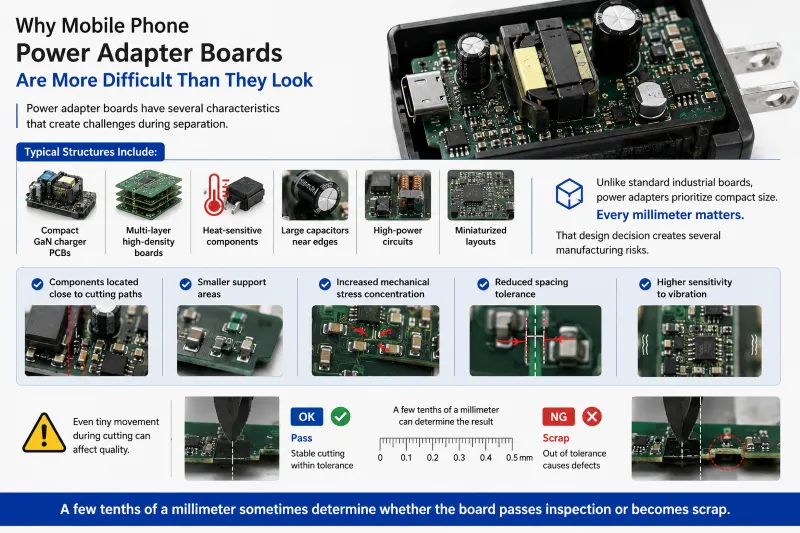
🔍 Why Mobile Phone Power Adapter Boards Are More Difficult Than They Look
Power adapter boards have several characteristics that create challenges during separation.
Typical structures include:
- Compact GaN charger PCBs
- Multi-layer high-density boards
- Heat-sensitive components
- Large capacitors near edges
- High-power circuits
- Miniaturized layouts
Unlike standard industrial boards, power adapters prioritize compact size.
Every millimeter matters.
That design decision creates several manufacturing risks.
- ✓ Components located close to cutting paths
- ✓ Smaller support areas
- ✓ Increased mechanical stress concentration
- ✓ Reduced spacing tolerance
- ✓ Higher sensitivity to vibration
Even tiny movements during cutting can affect quality.
A few tenths of a millimeter sometimes determine whether the board passes inspection or becomes scrap.
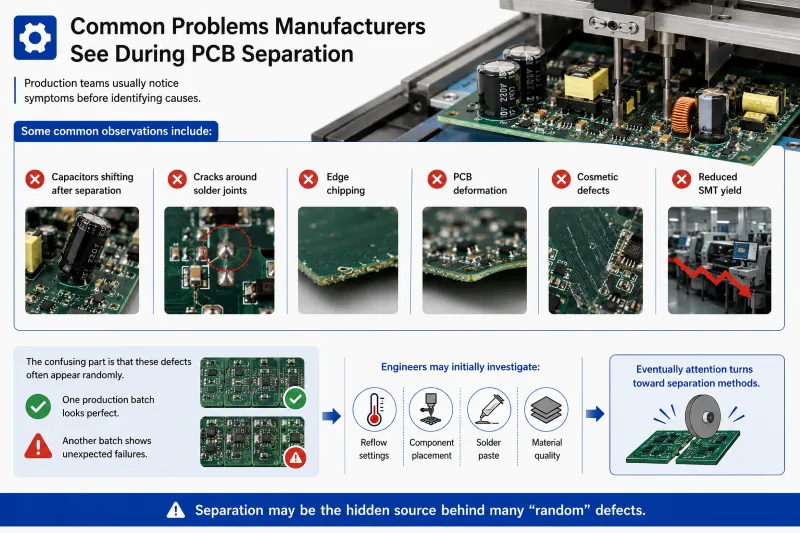
⚙️ Common Problems Manufacturers See During PCB Separation
Production teams usually notice symptoms before identifying causes.
Some common observations include:
- Capacitors shifting after separation
- Cracks around solder joints
- Edge chipping
- PCB deformation
- Cosmetic defects
- Reduced SMT yield
The confusing part is that these defects often appear randomly.
One production batch looks perfect.
Another batch shows unexpected failures.
Engineers may initially investigate:
- Reflow settings
- Component placement
- Solder paste
- Material quality
Eventually, attention turns toward separation methods.
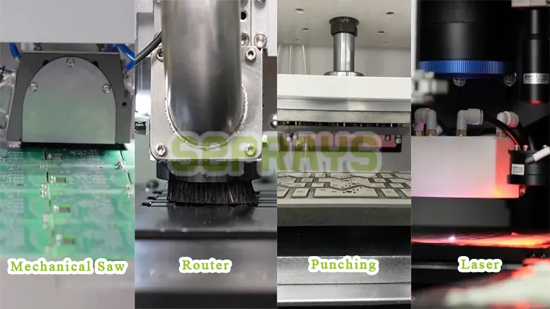
📊 Comparing Different Separation Methods for Power Adapter PCBs
| Separation Method | Mechanical Stress | Flexibility | 속도 | Suitable for Compact Power Adapter Boards |
|---|---|---|---|---|
| V-Groove | Medium–High | Low | High | Limited |
| Punching | High | 중소 | Very High | Not ideal |
| Laser Cutting | Very Low | Very High | 중소 | Good |
| 라우터 구분 | Low | High | High | Excellent |
For many manufacturers, router solutions provide a practical balance between cutting quality and production efficiency.
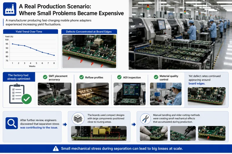
🏭 A Real Production Scenario: Where Small Problems Became Expensive
A manufacturer producing fast-charging mobile phone adapters experienced increasing yield fluctuations.
The factory had already optimized:
- ✓ SMT placement accuracy
- ✓ Reflow profiles
- ✓ AOI inspection
- ✓ Material quality control
Yet defect rates continued appearing around board edges.
After further review, engineers discovered that separation stress was contributing to the issue.
The boards used compact designs with large components positioned close to routing areas.
Manual handling and older cutting methods were creating small mechanical effects that accumulated during production.
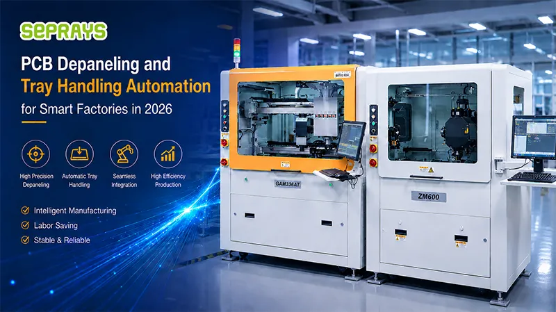
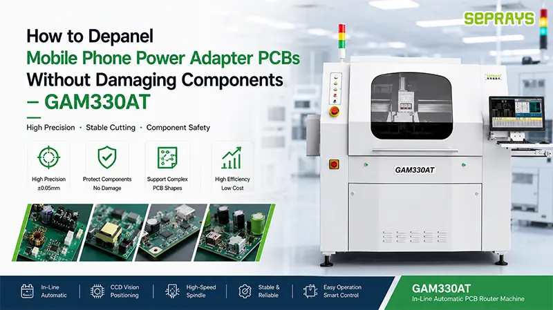
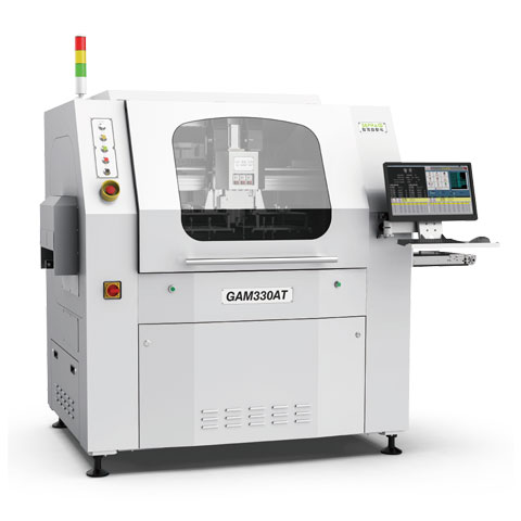
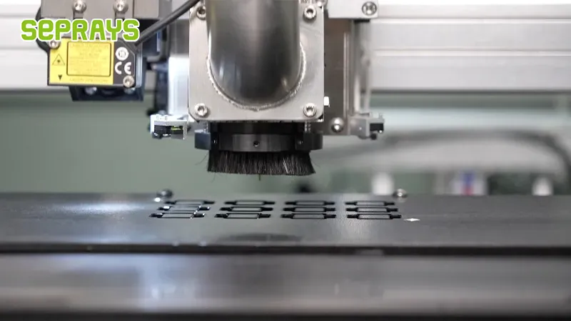
🛠 How GAM330AT Helped Improve Stability
The team later evaluated the Seprays GAM330AT In-Line Automatic PCB Router Machine.
The objective was not simply faster cutting.
The goal was better consistency.
Several functions became important:
- ✓ CCD vision positioning for accurate routing alignment
- ✓ Stable high-speed spindle operation
- ✓ Automated inline handling
- ✓ Reduced operator intervention
- ✓ Flexible routing capability for compact structures
Instead of relying heavily on manual positioning, the process became more repeatable.
Production output became easier to predict.
That matters more than many people realize.
A stable process often saves more money than a faster process.
💡 A Counterintuitive Observation from Production Floors
Many people assume:
“Smaller boards automatically require laser cutting.”
Not necessarily.
Laser systems can provide excellent precision.
But precision alone does not determine total production cost.
Manufacturers also consider:
- Production volume
- Maintenance requirements
- Throughput targets
- Future product variation
- Automation compatibility
For high-volume adapter production, routing systems often provide a better balance between investment and productivity.
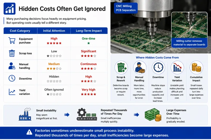
📈 Hidden Costs Often Get Ignored
Many purchasing decisions focus heavily on equipment pricing.
But operating costs usually tell a different story.
| Cost Category | Initial Attention | Long-Term Impact |
| Equipment purchase | High | One-time |
| Scrap loss | Low | Significant |
| Manual handling | 중소 | Continuous |
| Downtime | Hidden | High |
| Yield variation | Often ignored | Very high |
Factories sometimes underestimate small process instability.
Repeated thousands of times per day, small inefficiencies become large expenses.
🔧 Practical Selection Checklist Before Choosing a Depaneling Method
Before selecting equipment, manufacturers often review:
- ✓ Component distance from board edge
- ✓ Board thickness
- ✓ Daily output requirements
- ✓ Future product changes
- ✓ Automation needs
- ✓ Yield targets
- ✓ Maintenance requirements
Simple questions prevent expensive corrections later.
🌎 Looking Ahead in 2026
Mobile phone power adapter products continue moving toward:
- Smaller form factors
- Higher charging power
- More complex structures
- Higher output volumes
Depaneling is no longer viewed as only a cutting process.
Increasingly, it becomes part of an integrated manufacturing strategy.
The conversation is gradually changing from:
“Can the board be cut?”
to:
“Can the board be cut repeatedly without affecting quality?”
That difference matters.
Why Choose Seprays Group?
For more than 30 years, Seprays Group has continuously developed PCB depaneling technologies for evolving manufacturing environments.
Seprays Group has been dedicated to PCB/FPC depaneling technology, providing a full range of solutions—including milling-cutter, laser, V-groove, and punching depanelers, as well as automated handling systems.
Our solutions are trusted by leading manufacturers, including Foxconn, Flextronics, State Grid, Luxshare, Compal, Wistron, China Electronics, Quanta, CRRC, China Aerospace, OPPO, ZTE, and Bosch, supporting production facilities across China and worldwide.
We focus not only on equipment performance but also on:
- ✓ Production process optimization
- ✓ Stable automation integration
- ✓ Long-term operating reliability
- ✓ Flexible manufacturing support
- ✓ Industry-specific solutions
If you are evaluating PCB depaneling solutions for mobile phone power adapter production, please feel free to contact us.
WhatsApp: +8618929266433
이메일: sales@seprays.com
FAQ
1. Why are mobile phone power adapter PCBs difficult to depanel?
Because modern adapter boards often have compact layouts with components located very close to board edges.
2. Can router depaneling damage nearby components?
With proper support design and optimized routing parameters, mechanical stress can be significantly reduced.
3. Is GAM330AT suitable for high-volume production?
Yes. Its inline design supports automated workflows and continuous production environments.
4. Should all compact adapter boards use laser cutting?
No. The best method depends on volume, structure, budget, and production requirements.
5. What is the highest hidden cost during PCB separation?
Yield instability and repeated small process interruptions often result in long-term costs that exceed the equipment purchase price.