.png)
 Russian
  English
  Spanish
  Japanese
  Korean
  Chinese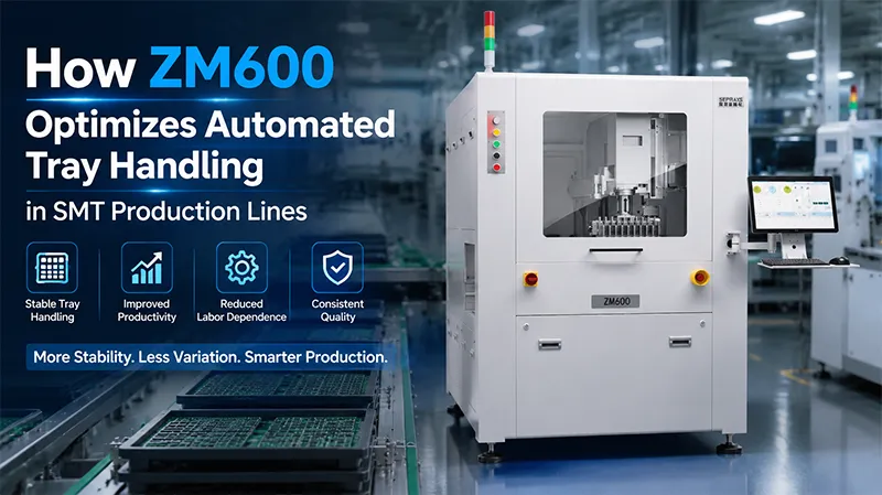
How ZM600 Optimizes Automated Tray Handling in SMT Production Lines
ZM600 automated tray handling was developed from a simple production reality: in modern SMT factories, the process after PCB assembly can become just as important as the assembly process itself. Many manufacturers invest heavily in high-speed placement machines, advanced inspection systems, and intelligent production software. But one question is often overlooked: What happens when finished boards need to be transferred, loaded, and managed between processes? In many factories, tray handling still depends on manual operations or semi-automatic solutions. At low production volumes, this may appear acceptable. However, when production scales up, small variations begin to create larger problems. Operators spend more time adjusting trays. Production flow becomes less predictable. Traceability becomes harder. And the hidden labor cost continues increasing. This is where automated tray handling becomes a practical manufacturing discussion. 🔍 Why SMT Production Lines Started Facing Tray Handling Challenges Traditional SMT production environments were designed around simpler workflows. Products had: Modern electronics manufacturing has changed significantly. Factories today increasingly produce: These applications introduce new requirements: The challenge is not only placing components accurately. The entire production chain needs to remain stable. A perfectly assembled PCB can still experience problems if handling between processes is inconsistent. ⚠️ Common Questions SMT
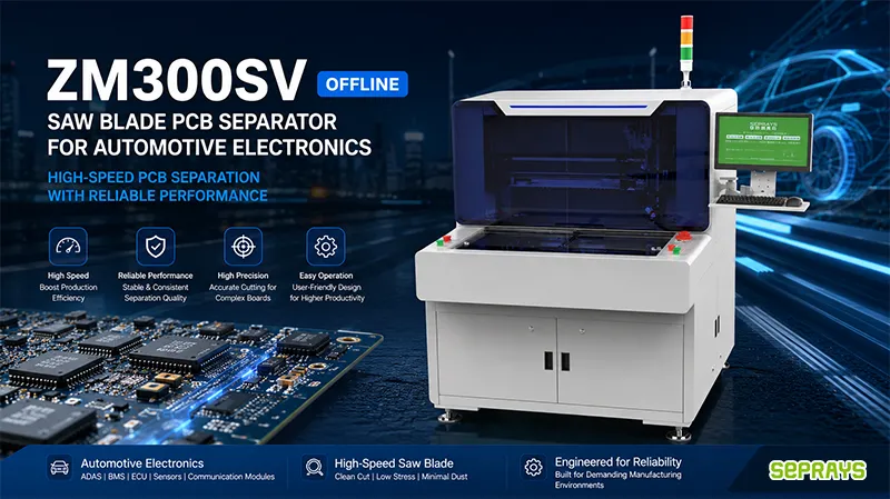
ZM300SV Offline Saw Blade PCB Separator for Automotive Electronics: High-Speed PCB Separation with Reliable Performance
ZM300SV Offline Saw Blade PCB Separator for Automotive Electronics is becoming a more common discussion point among production engineers dealing with compact automotive electronics. A few years ago, many PCB separation tasks were relatively straightforward. Larger boards allowed more process tolerance. Small process deviations rarely caused major concerns. That situation changed quickly. Modern automotive electronics continue moving toward smaller dimensions, denser component layouts, and stricter reliability requirements. The challenge is no longer simply separating boards faster. The challenge is doing it repeatedly, consistently, and without introducing hidden quality risks. Interestingly, many production teams discover this only after defects begin appearing later in the process. 🔍 Why Automotive Electronics Changed PCB Separation Requirements Automotive electronics introduced a very different manufacturing environment. Current applications increasingly involve: Several manufacturing issues often arrive together: At first glance, these products seem smaller and easier to process. Reality often proves the opposite. Smaller boards frequently create larger manufacturing risks. A difference of only 0.2–0.3 mm may determine whether a board remains stable after long-term vibration testing. ⚠️ Questions Production Teams Keep Asking Inside automotive factories, similar conversations repeat across projects: “Why did the board pass functional testing but fail environmental testing?” “Why do defect rates rise
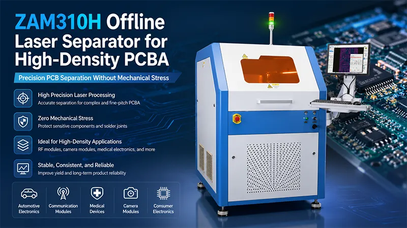
ZAM310H Offline Laser Separator for High-Density PCBA: Precision PCB Separation Without Mechanical Stress
ZAM310H Offline Laser Separator for High-Density PCBA is becoming a more practical topic inside electronics manufacturing discussions in 2026. A few years ago, engineers could tolerate small process variation because PCB layouts were less crowded and component spacing was more forgiving. That situation changed. Today’s products continue to become smaller while expectations for reliability continue to rise. Consumer devices are thinner. Automotive modules contain more functions. Medical electronics require greater stability. RF communication boards integrate more sensitive structures into smaller spaces. Interestingly, the challenge is not simply cutting a PCB anymore. The larger challenge is preventing invisible damage that appears weeks later. Many engineers discover this only after unexpected field failures start appearing. 🔍 Why High-Density PCBA Changed PCB Separation Requirements Traditional PCB assemblies provided larger process windows. Modern products have reduced those margins dramatically. Today, manufacturers increasingly work with: Several manufacturing problems often appear simultaneously: The surprising part: Smaller products often create larger production risks. A difference of only a few tenths of a millimeter can determine whether products pass long-term reliability testing. ⚠️ Common Questions Production Teams Continue Asking Inside factories across different industries, conversations often sound surprisingly similar: “Why do boards pass electrical testing but later fail
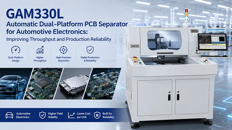
GAM330L Automatic Dual-Platform PCB Separator for Automotive Electronics: Improving Throughput and Production Reliability
GAM330L Automatic Dual-Platform PCB Separator technology is becoming a larger discussion point inside automotive electronics manufacturing in 2026. The reason is not simply speed. Production teams increasingly face a different challenge: maintaining stable quality while output continues growing. Several years ago, separating automotive PCBA panels was often considered a standard process step. Today, it increasingly affects long-term reliability, production cost, and yield consistency. As vehicle electronics continue evolving toward ADAS systems, battery management modules, vehicle communication units, and intelligent sensors, manufacturers are discovering that separation quality directly influences product performance. A small crack created during cutting may not appear immediately. Sometimes it appears months later. That is where production concerns start becoming expensive. 🔍 Why Automotive Electronics Create Different Manufacturing Challenges Traditional PCB products often had more flexibility. Automotive electronics changed the rules. Modern automotive applications increasingly include: Several manufacturing challenges frequently appear together: The interesting part is that many automotive boards look relatively small. Ironically, smaller boards often create larger production problems. Because there is less space for error. Sometimes only fractions of a millimeter separate a stable product from a future field failure. ⚠️ Common Questions Production Teams Keep Asking Inside automotive manufacturing environments, similar discussions happen repeatedly:
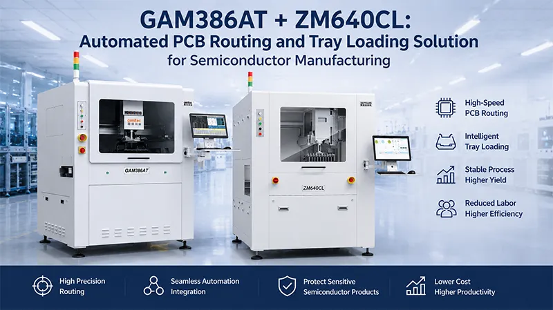
GAM386AT + ZM640CL: Automated PCB Routing and Tray Loading Solution for Semiconductor Manufacturing
Automated PCB routing and tray loading solutions are becoming a much larger topic inside semiconductor factories than they were just a few years ago. In conversations with production engineers, the discussion is no longer only about cutting precision. More often, it starts with questions like: “How can we reduce operator dependency?” “How can we avoid micro-damage during high-volume production?” “How can routing and material handling work as one process instead of two separate steps?” Semiconductor manufacturing in 2026 is changing quickly. Package sizes continue shrinking. Product cycles continue to shorten. Yield expectations continue increasing. Ironically, smaller products are creating bigger manufacturing challenges. 🔍 Why Semiconductor Production Is Creating New Challenges Traditional PCB production environments had more flexibility. Boards were larger. Component spacing was wider. Manual intervention was more acceptable. Modern semiconductor applications changed that environment. Current production increasingly includes: Several manufacturing difficulties often appear simultaneously: The challenge becomes even larger when routing and handling happen as isolated operations. A perfectly cut board can still become damaged during transfer. That point is often overlooked. ⚠️ Common Questions Production Teams Keep Asking Across different semiconductor factories, engineers often discuss surprisingly similar problems: “Why do some boards pass inspection but later show random
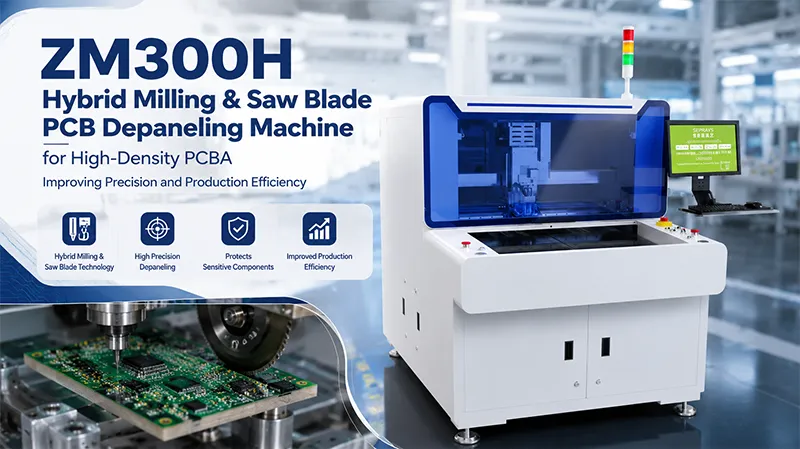
ZM300H Hybrid Milling & Saw Blade PCB Depaneling Machine for High-Density PCBA: Improving Precision and Production Efficiency
ZM300H Hybrid Milling & Saw Blade PCB Depaneling Machine for High-Density PCBA became a frequent topic in production meetings for a simple reason: PCB designs changed faster than many manufacturing processes could keep up with. Several years ago, separating PCBs was often considered a straightforward step. Panels were larger. Components had more spacing. Production tolerances were relatively forgiving. Today, that assumption no longer holds. In 2026, manufacturers of automotive electronics, communication modules, wearable products, industrial control systems, and compact consumer devices are operating in a different environment. Boards continue getting smaller. Components continue moving closer to PCB edges. Yet quality expectations continue rising. Many engineers have discovered an uncomfortable reality: The cutting process itself often becomes one of the final hidden variables affecting yield. 🔍 Why High-Density PCBA Creates New Challenges Traditional PCB structures offered more room for process variation. High-density assemblies change everything. Modern production increasingly includes: Several problems often appear together: The challenge becomes greater when components are positioned extremely close to board edges. In many cases, fractions of a millimeter determine whether boards pass inspection or require rework. Ironically, smaller electronics often create larger manufacturing problems. ⚠️ Common Questions Manufacturing Teams Continue Asking Conversations inside different factories